Supercharge Your Innovation With Domain-Expert AI Agents!

Micro-Modules with Molded Passive Components, Systems Using the Same, and Methods of Making the Same

a technology of passive components and micro-modules, which is applied in the direction of electrical apparatus, semiconductor devices, semiconductor/solid-state device details, etc., can solve the problems of increasing the design, size and assembly requirements of interconnect substrates, increasing the demand for a smaller form factor, and increasing so as to increase the functionality and features of electronic products, increase the area and cost of substrates, and reduce the effect of product yield

Inactive Publication Date: 2009-12-24
SEMICON COMPONENTS IND LLC
View PDF18 Cites 14 Cited by
  • Summary
  • Abstract
  • Description
  • Claims
  • Application Information

AI Technical Summary

Benefits of technology

The invention is about a way to make electronic products with more features without increasing their size or cost. It involves combining components of a circuit into a single package, which reduces the space required for the circuit. This allows for the creation of ultra-miniature power converters and other circuits that can be used in portable consumer products. The invention also includes a method of manufacturing the semiconductor die package and a system with the package attached to an interconnect substrate. Overall, the invention enables the creation of smaller, more powerful electronic products.

Problems solved by technology

This, in turn, has placed ever increasing demands on the design, size, and assembly of the interconnect substrates.
As the number of assembled components increases, substrate areas and costs increase, while demand for a smaller form factor increases.

Method used


Image

  • Micro-Modules with Molded Passive Components, Systems Using the Same, and Methods of Making the Same
  • Micro-Modules with Molded Passive Components, Systems Using the Same, and Methods of Making the Same
  • Micro-Modules with Molded Passive Components, Systems Using the Same, and Methods of Making the Same

Examples


Embodiment Construction

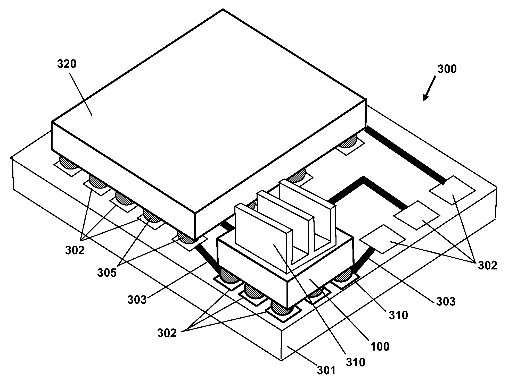
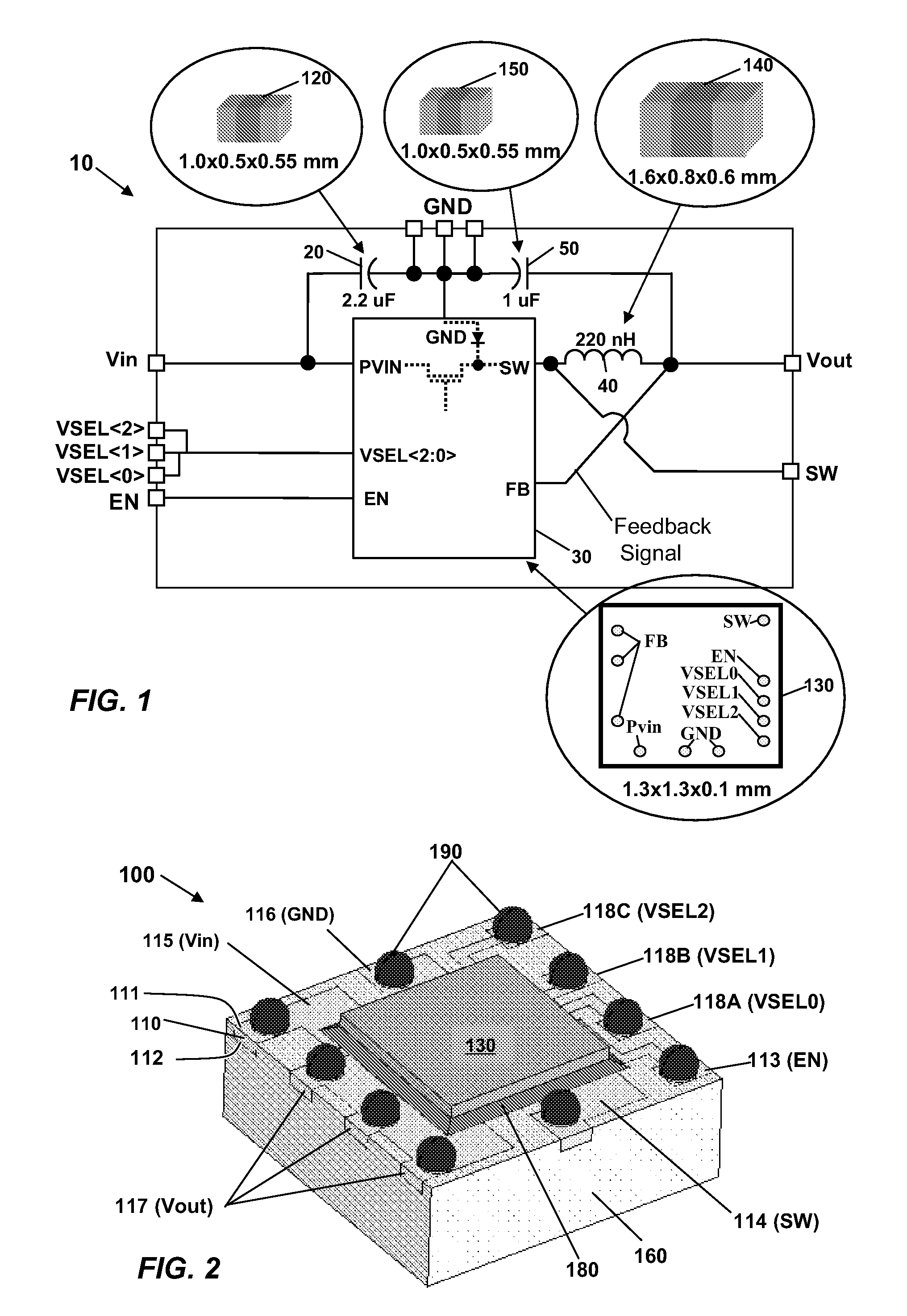
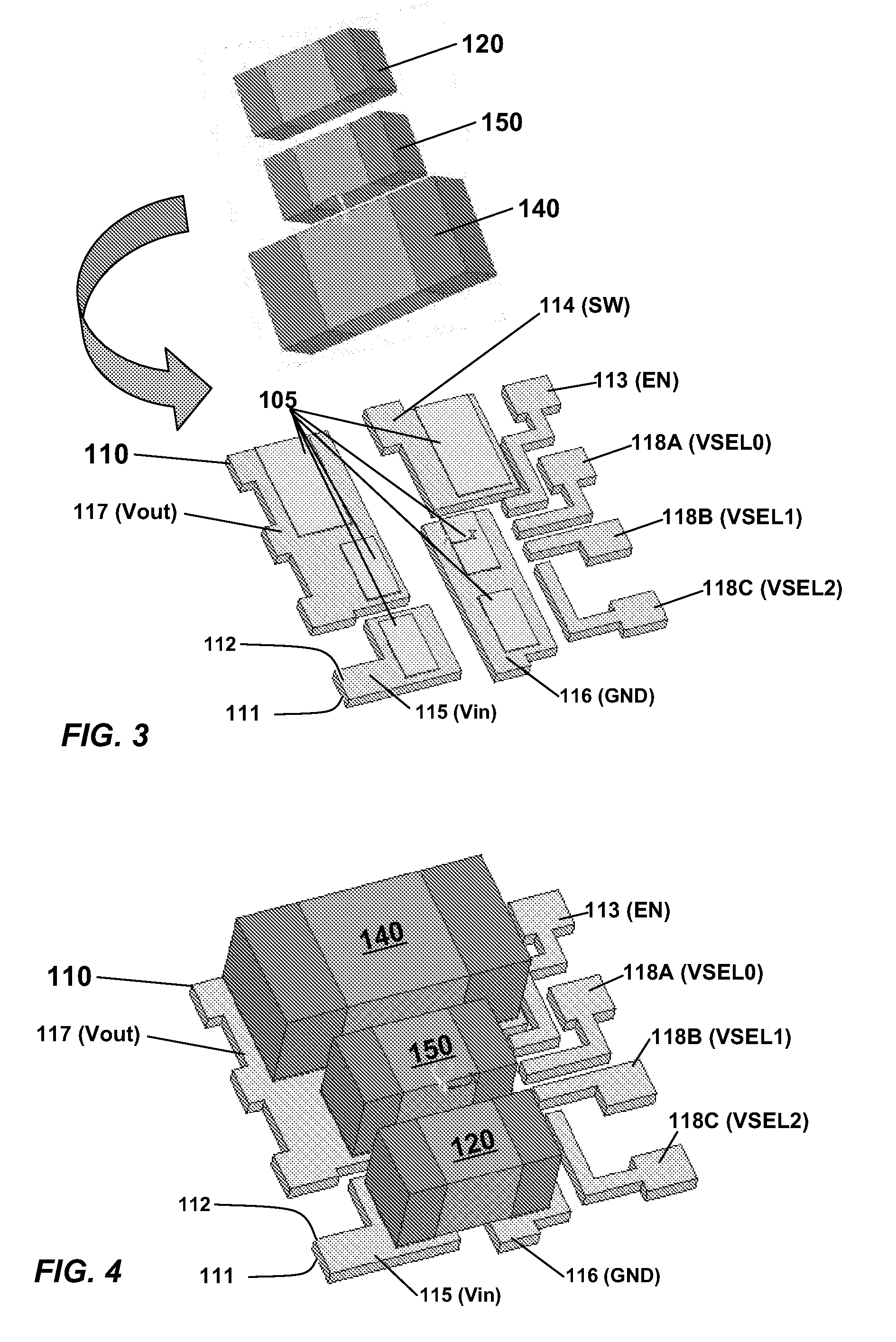
[0014]FIG. 1 shows a schematic diagram of an exemplary circuit group 10 that may be incorporated into a package according to the present invention. For illustration purposes, and without loss of generality, circuit group 10 may comprise a power conversion circuit that receives input power provided between an input voltage terminal Vin and ground terminal GND, and generates an output power supply at a different voltage level between an output terminal Vout and the ground terminal GND. Circuit group 10 includes various control inputs provided at terminals EN and VSEL2:0>. Circuit group 10 includes an input capacitor 20 coupled between the Vin and GND terminals, a power regulator circuit 3030 coupled between input capacitor 20 and a switch terminal SW, an inductor 40 coupled between the SW and Vout terminals, and an output capacitor 50 coupled between the Vout and GND terminals. Capacitor 20 may be implemented by a surface-mount capacitor 120, regulator circuit 30 may be implemented by...


PUM


Abstract

Semiconductor die packages, methods of making said packages, and systems using said packages are disclosed. An exemplary package comprises at least one semiconductor die disposed on one surface of a leadframe and electrically coupled to at least one conductive region of the leadframe, and at least one passive electrical component disposed on the other surface of a leadframe and electrically coupled to at least one conductive region of the leadframe. Molding material is disposed over the at least one passive electrical component to provide a molded passive component.

Description

CROSS-REFERENCES TO RELATED APPLICATIONS[0001]NOT APPLICABLEBACKGROUND OF THE INVENTION[0002]Personal electronic products, such as cell phones, personal data assistants, digital cameras, laptops, etc, are generally comprised of several packaged semiconductor IC chips and surface mount components assembled onto interconnect substrates, such as printed circuit boards and flex substrates. There is an ever increasing demand to incorporate more functionality and features into personal electronic products and the like. This, in turn, has placed ever increasing demands on the design, size, and assembly of the interconnect substrates. As the number of assembled components increases, substrate areas and costs increase, while demand for a smaller form factor increases.BRIEF SUMMARY OF THE INVENTION[0003]As part of making their invention, the inventors have recognized that there is a need to address these issues and that it would be advantageous to find ways to enable increases in functionalit...

Claims


Application Information

Patent Timeline
Patent Type & Authority Applications(United States)
IPC IPC(8): H01L23/495H01L21/56
CPCH01L21/56H01L21/563H01L23/3107H01L23/49589H01L23/498H01L2924/19041H01L23/5222H01L2224/73203H01L2924/01079H01L2924/13091H01L23/49861
Inventor LIU, YONGLIU, YUMINJOHNSON, TERRYHAWKS, DOUG
Owner SEMICON COMPONENTS IND LLC
Features
  • R&D
  • Intellectual Property
  • Life Sciences
  • Materials
  • Tech Scout
  • Unparalleled Data Quality
  • Higher Quality Content
  • 60% Fewer Hallucinations
Learn More