Image sensor and fabricating method thereof

a technology of image sensor and manufacturing method, which is applied in the field of image sensor, can solve the problems of reducing the image affecting the quality of the cmos image sensor, and peeling of the color filter unit in the color filter array, so as to achieve the effect of effectively removing the under layer

Active Publication Date: 2009-12-31
UNITED MICROELECTRONICS CORP
View PDF5 Cites 21 Cited by
  • Summary
  • Abstract
  • Description
  • Claims
  • Application Information

AI Technical Summary

Benefits of technology

[0009]Accordingly, the present invention provides a method for fabricating

Problems solved by technology

However, many problems still exist in the processes of fabricating CMOS image sensors, and they impair the quality of CMOS image sensors.
It is noted that, when a photoresist material is applied to form the color filter array, the opening exposing the pad will cause the uneven coating or residuals of the photoresist material, which reduces the image quality of the CMOS image se

Method used


Image

  • Image sensor and fabricating method thereof
  • Image sensor and fabricating method thereof
  • Image sensor and fabricating method thereof

Examples


Embodiment Construction

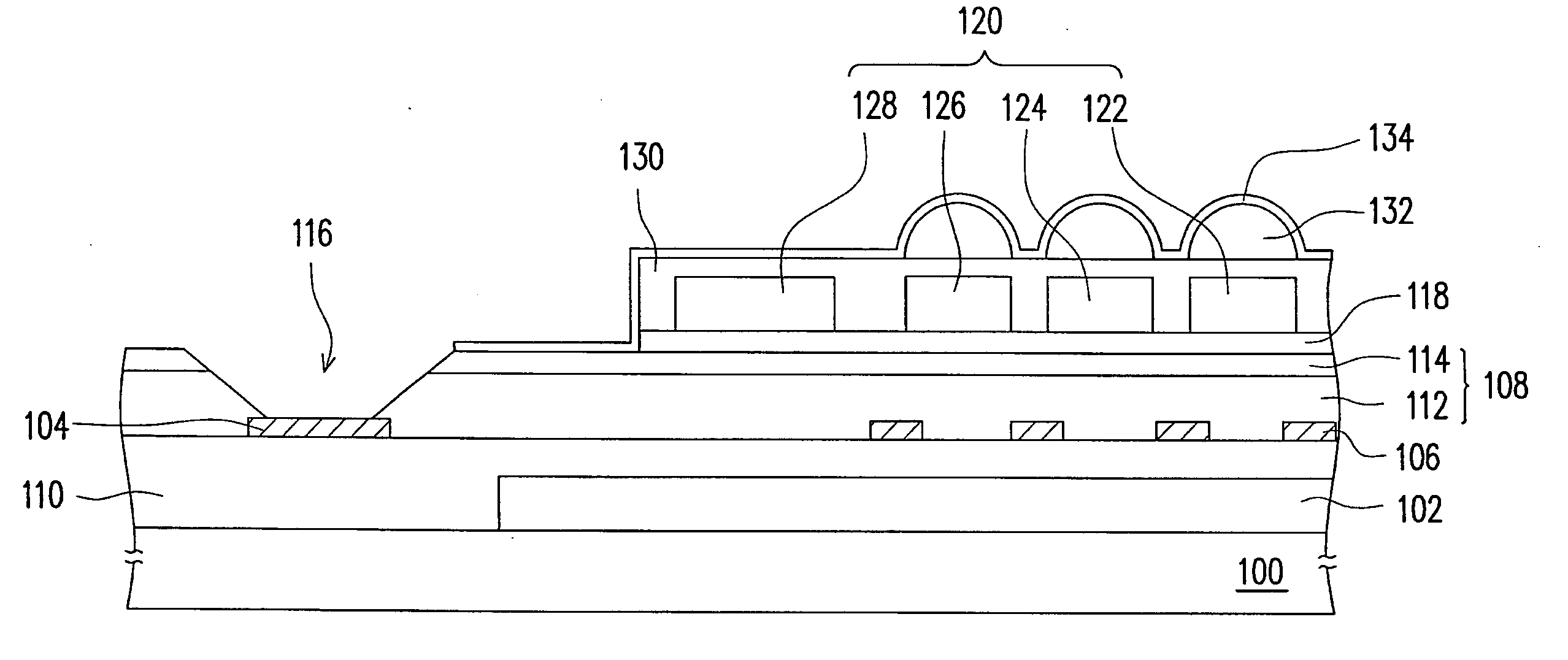
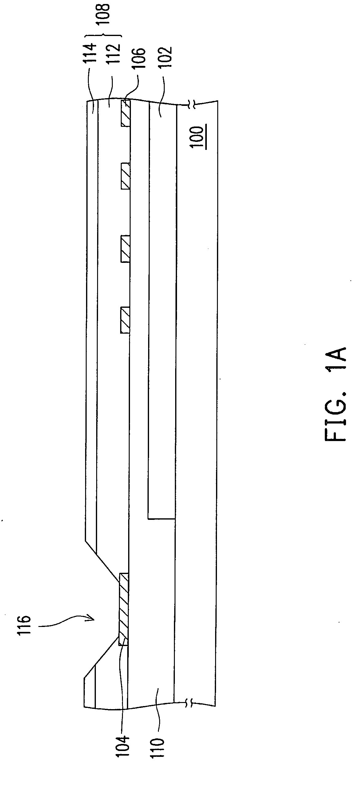
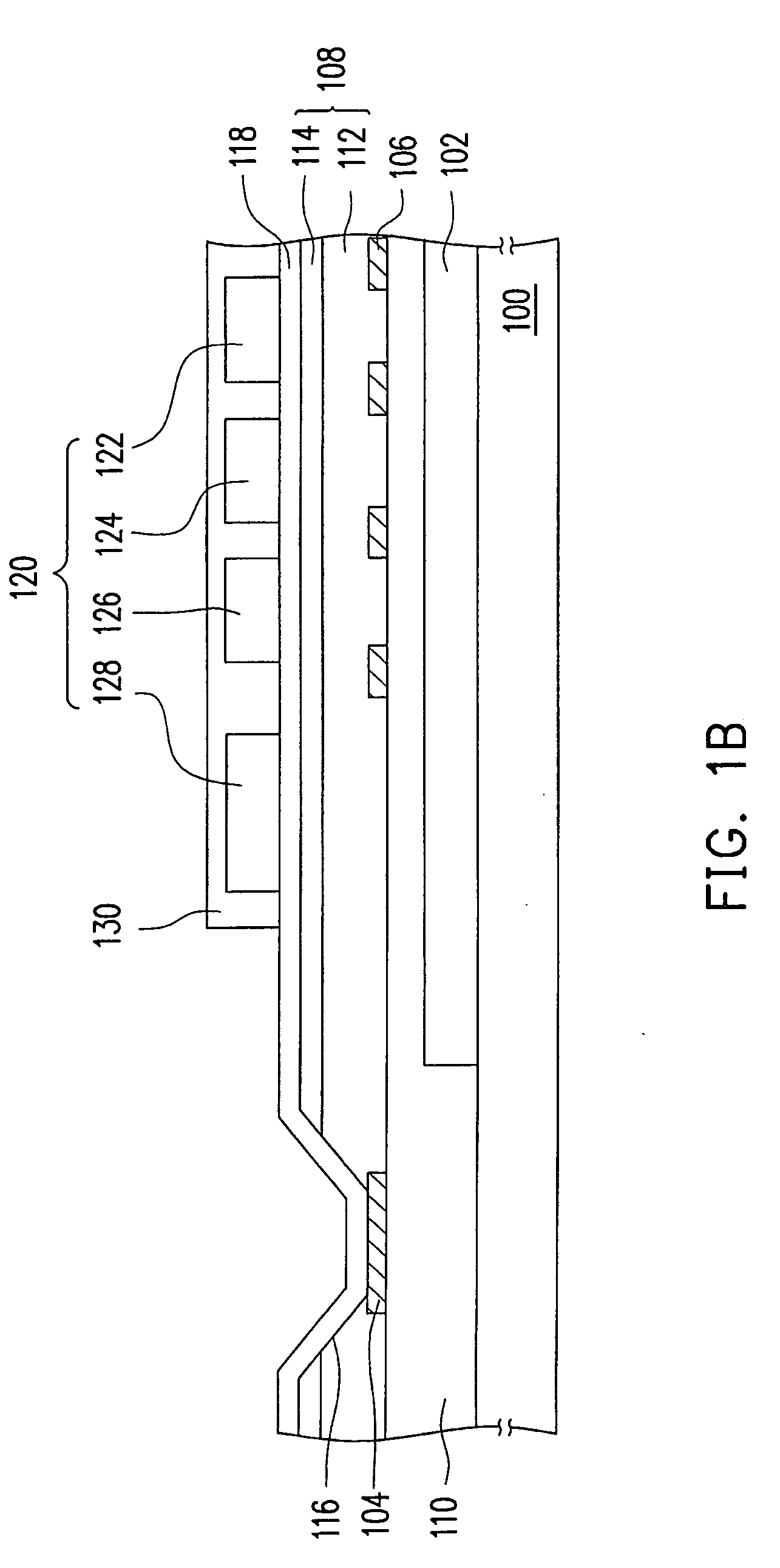
[0039]FIGS. 1A through 1C are schematic cross-sectional views illustrating a process flow for fabricating an image sensor according to an embodiment of the present invention.

[0040]First, referring to FIG. 1A, a semiconductor substrate 100, such as a silicon substrate, is provided. The semiconductor substrate 100 comprises a sensor array 102 (schematic diagram), a pad 104, a patterned metal layer 106, and a passivation layer 108.

[0041]The sensor array 102 is formed in a sensor array layer 110, for example. The sensor array 102 is formed by a plurality of photosensitive diodes (not shown), for example. The photosensitive diodes, for example, comprise CMOS transistors (not shown) and photosensitive areas (not shown), and the CMOS transistors and the photosensitive areas are electrically connected with each other.

[0042]The pad 104 and the patterned metal layer 106 are, for example, formed on the sensor array layer 110. The pad 104 is formed outside an area of the sensor array 102 for wi...


PUM


Abstract

A method for fabricating an image sensor, which includes the following steps, is provided. A semiconductor substrate including a sensor array, a pad and a passivation layer is provided, and the passivation layer covers the sensor array and the pad. An opening, which comprises tapered sidewalls not perpendicular to a bared surface of the pad, is formed in the semiconductor substrate to expose the pad. An under layer is formed on the semiconductor substrate, and covers the pad and the passivation layer. A color filter array is formed on the under layer and over the corresponding sensor array. A planar layer is formed on the color filter array. A portion of the under layer is removed to expose the pad. A plurality of U-lenses is formed on the planar layer.

Description

BACKGROUND OF THE INVENTION[0001]1. Field of the Invention[0002]The present invention relates to a semiconductor device and a fabricating method thereof, and particularly relates to an image sensor and a fabricating method thereof.[0003]2. Description of Related Art[0004]An image sensor is an electronic device, which converts optical information into electrical signals. Image sensors are roughly divided into two different categories, Cathode Ray Tube (CRT) and fixed photograph device. CRT is mainly applied in television (TV) and widely used for applying image processing techniques in measuring, controlling, and recognizing application techniques. At present, there are two types of fixed photograph devices, including a charged coupled device (CCD) and a complementary metal-oxide-semiconductor (CMOS).[0005]A complementary metal-oxide-semiconductor (CMOS) image sensor is a device, which converts optical images into electrical signals through CMOS fabricating technique. Compared with a ...

Claims


Application Information

Patent Timeline
IPC IPC(8): H01L31/0232H01L31/18
CPCH01L27/14621H01L27/14632H01L27/14627
Inventor YU, CHENG-HUNG
Owner UNITED MICROELECTRONICS CORP
Why Eureka
Try Eureka