Organic light emitting diode display and method of manufacturing the same

a technology of light-emitting diodes and organic light-emitting diodes, which is applied in the direction of discharge tube luminescnet screens, sustainable manufacturing/processing, and final product manufacturing, etc., can solve the problems of large thickness of oled displays, deterioration of refractive properties, and deterioration of visual quality of images displayed by oled displays. , to achieve the effect of improving the productivity of oled displays and minimizing the thickness o

Active Publication Date: 2009-12-31
SAMSUNG DISPLAY CO LTD
View PDF16 Cites 58 Cited by
  • Summary
  • Abstract
  • Description
  • Claims
  • Application Information

AI Technical Summary

Benefits of technology

[0030]Furthermore, the entire thickness of the OLED display can be minimized.
[0031]In addition, productiv

Problems solved by technology

Therefore, there is a problem in that visibility of an image which is displayed by the OLED display is deteriorated due to a difference in refractive indexes of the cover window and the separation space, deterioration of a refractive index due to the separation space,

Method used


Image

  • Organic light emitting diode display and method of manufacturing the same
  • Organic light emitting diode display and method of manufacturing the same
  • Organic light emitting diode display and method of manufacturing the same

Examples


Embodiment Construction

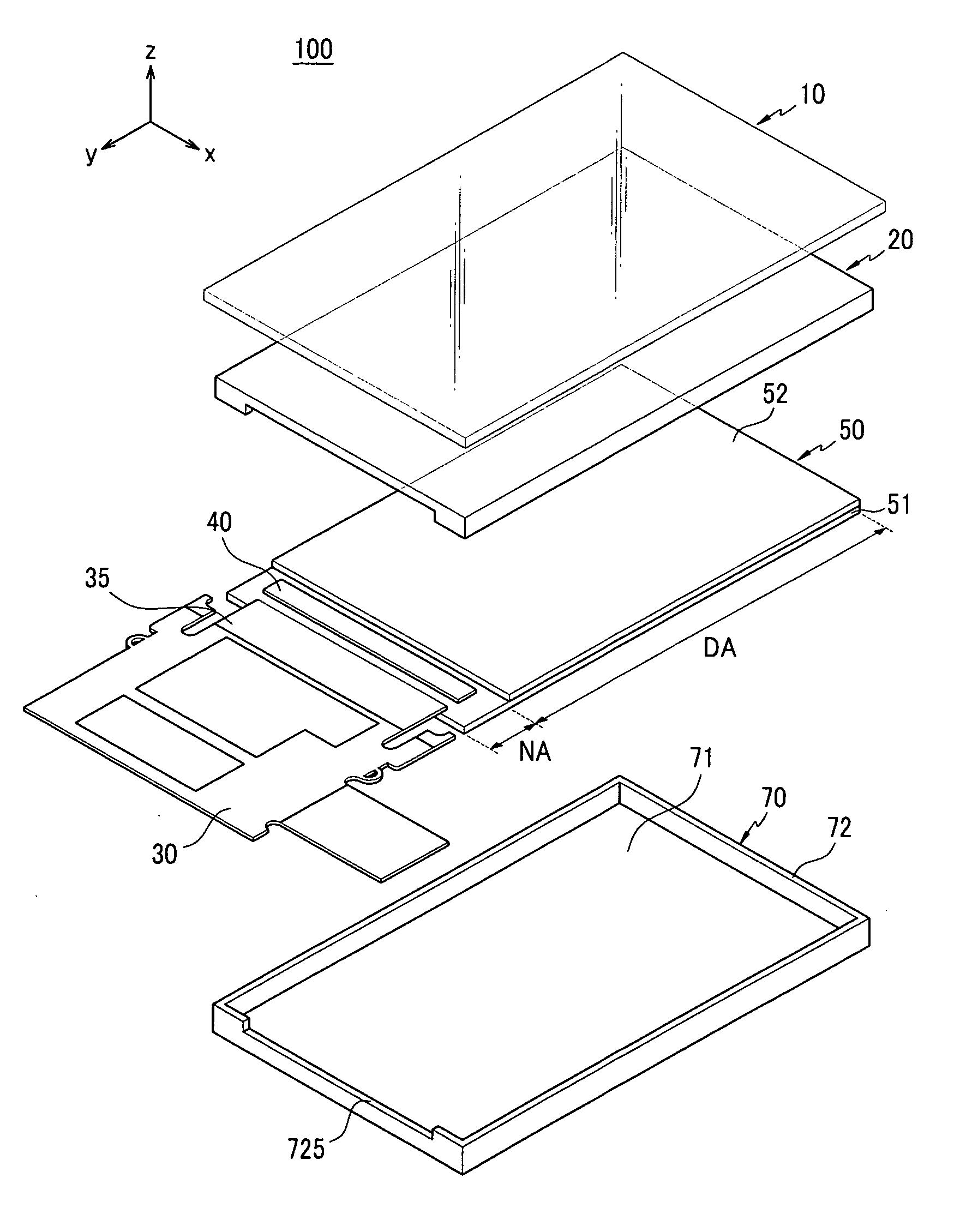
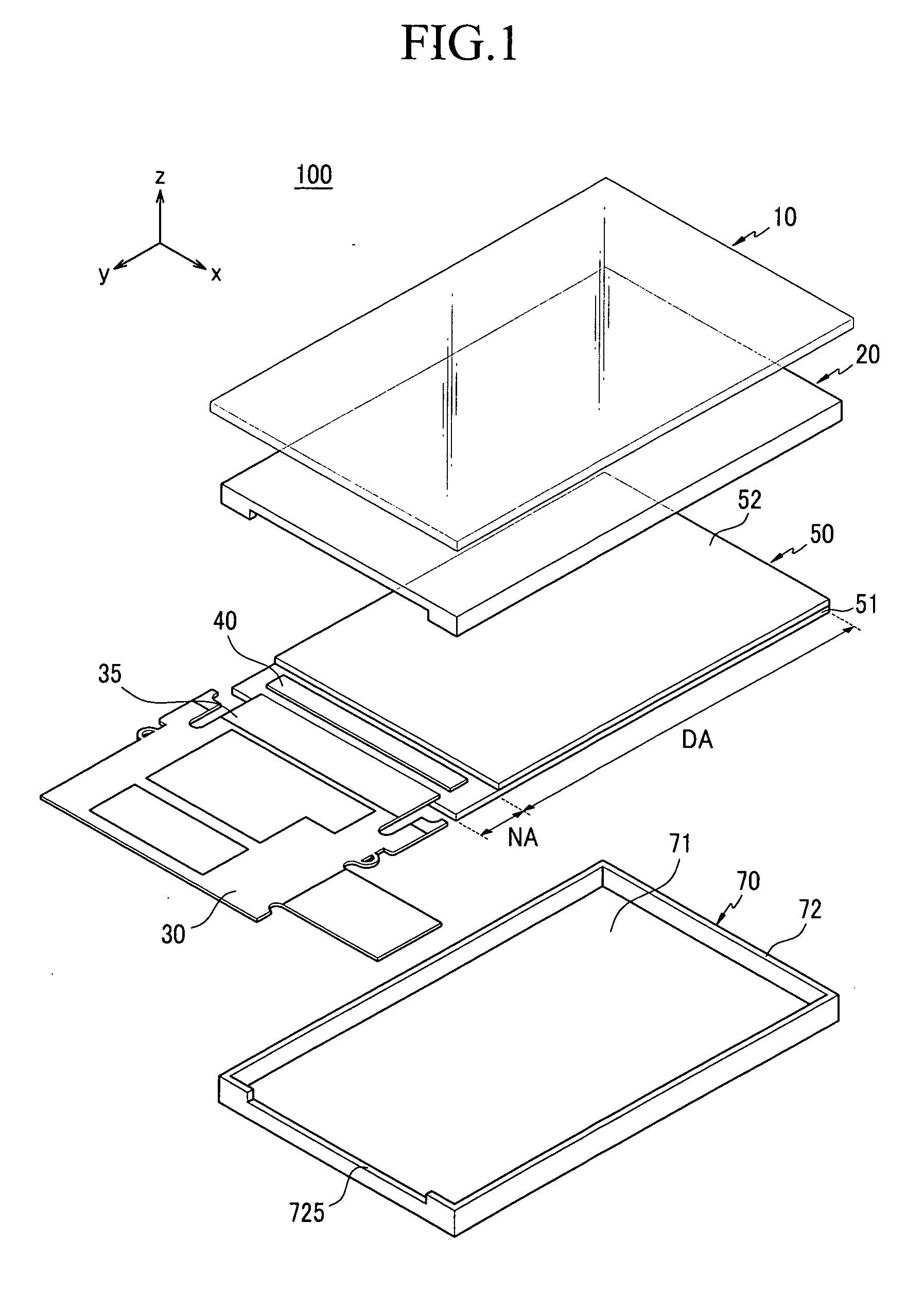
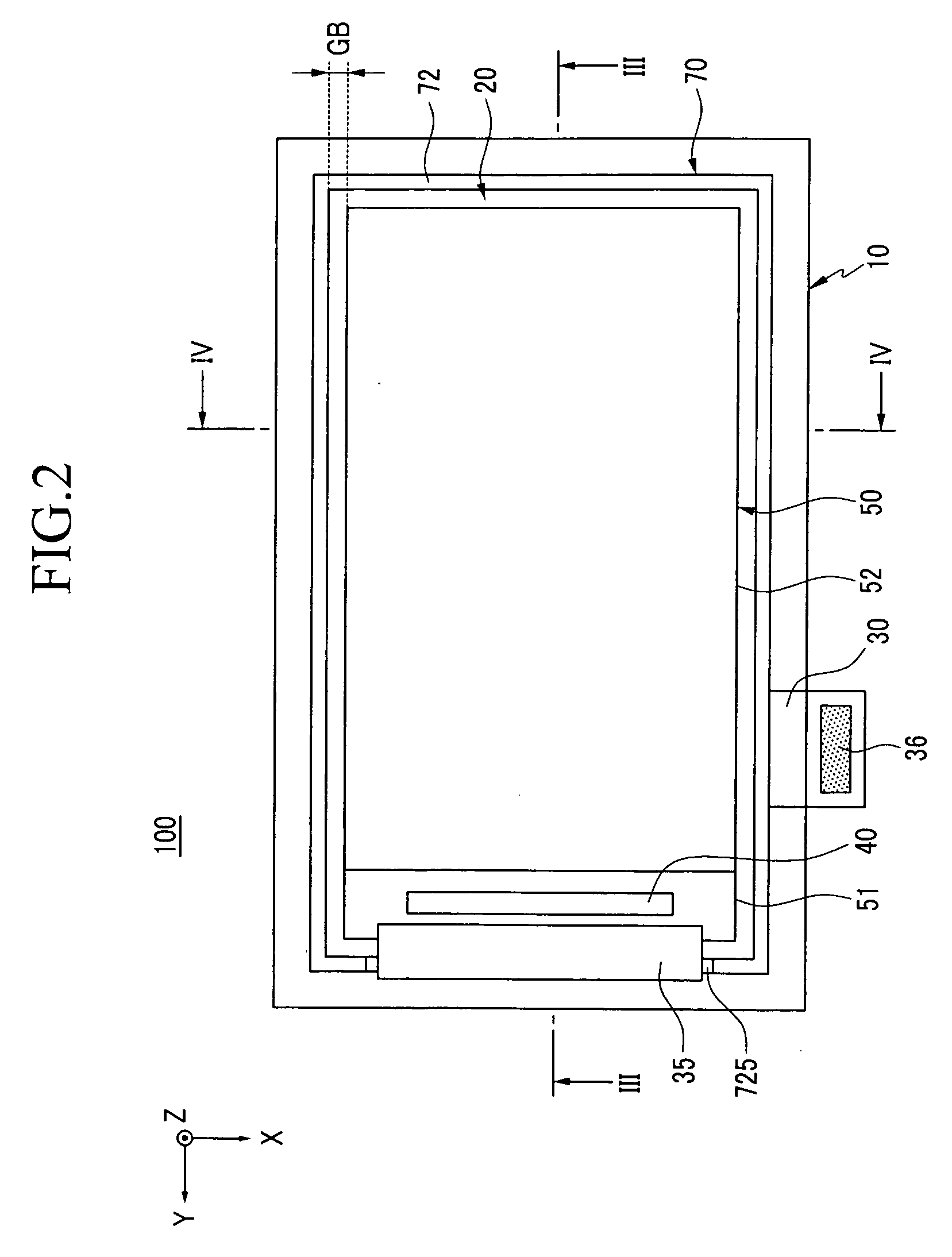
[0041]The present invention will be described more fully hereinafter with reference to the accompanying drawings, in which exemplary embodiments of the invention are shown. The present invention is not limited to the exemplary embodiments, but may be embodied in various forms.

[0042]Furthermore, because the size and thickness of each element displayed in the drawings are randomly displayed for better understanding and ease of description, the present invention is not limited thereto.

[0043]Accordingly, the drawings and description are to be regarded as illustrative in nature and not restrictive. Like reference numerals designate like elements throughout the specification.

[0044]In addition, in the drawings, the thickness of layers, films, panels, regions, etc., are exaggerated for clarity. Like reference numerals designate like elements throughout the specification. It will be understood that, when an element such as a layer, film, region or substrate is referred to as being “on” anoth...


PUM


Abstract

An organic light emitting diode (OLED) display and a method of manufacturing the same are provided. The OLED display includes: a display panel assembly including a first substrate having a display area and a mounting area, a second substrate coupled to the display area of the first substrate, and an integrated circuit chip mounted in the mounting area of the first substrate; a cover window disposed opposite the second substrate and the integrated circuit chip and covering the display panel assembly; and an adhesive layer which fills up a space between the second substrate and the cover window, and a space between the mounting area of the first substrate and the cover window.

Description

CLAIM OF PRIORITY[0001]This application makes reference to, incorporates the same herein, and claims all benefits accruing under 35 U.S.C. §119 from an application earlier filed in the Korean Intellectual Property Office on the 29th of June 2008 and there duly assigned Serial No. 10-2008-0061125.BACKGROUND OF THE INVENTION[0002]1. Field of the Invention[0003]The present invention relates to an organic light emitting diode (OLED) display and a method of manufacturing the same. More particularly, the present invention relates to an OLED display and a method of manufacturing the same in which stability and reliability of a display panel assembly are improved.[0004]2. Description of the Related Art[0005]An organic light emitting diode (OLED) display includes a plurality of organic light emitting diodes having a hole injection electrode, an organic emission layer, and an electron injection electrode. The OLED display emits light by energy which is generated when excitons, which are gener...

Claims


Application Information

Patent Timeline
IPC IPC(8): H01J1/62H01J9/00
CPCH05B33/04H01L51/524Y02E10/549Y02P70/50H10K50/841H01L2224/80874H01L2224/80862H10K77/111
Inventor LEE, DUK-JINKWAK, NOH-MINJUNG, WOO-SUKPARK, SANG-HUNJUNG, KYU-HO
Owner SAMSUNG DISPLAY CO LTD
Why Eureka
Try Eureka