Performance improvement of antennas

a technology of performance improvement and antenna, applied in the direction of antennas, antenna details, antenna earthings, etc., can solve the problems of large total efficiency, difficult to achieve the required impedance match and efficiency, and compact design of (internal) antennas, etc., to increase the operation bandwidth, increase the electrical length of the chassis, and increase the bandwidth effect of impedance and efficiency

Inactive Publication Date: 2009-12-31
NOKIA CORP
View PDF7 Cites 44 Cited by
  • Summary
  • Abstract
  • Description
  • Claims
  • Application Information

AI Technical Summary

Benefits of technology

[0021]Accordingly, by placing natural or artificial low-loss magnetic material on the ground plane or chassis of the antenna arrangement of e.g. a portable electronic device, the electrical length of the chassis can be increased (resonant frequency decreased) and matched or set closer to that of the antenna arrangement, which may increase the operation bandwidth (both impedance and efficiency bandwidth) of the antenna-chassis combination. This measure, in turn, can lead to a considerable increase in bandwidth. This effect can be further increased when combining at least one slot and at least one magnetic element covering the same at least partially. The increase of the electrical length enables a performance improvement of small antennas used in fairly small radio devices such as mobile phones or mobile terminals. Thus, the antenna arrangement is useful for such small radio devices.
[0022]The proposed solution is very simple to use and does not require making any slots or holes to the circuit board or chassis. Hence, signal lines inside the circuit board are not affected.

Problems solved by technology

However, when the length of the chassis is decreased below a certain size, e.g. 100 mm, it becomes difficult to design compact (internal) antennas that have sufficient impedance match and hence sufficiently large total efficiency to cover desired frequency ranges, such as both 850 MHz (824-894 MHz) and 900 MHz (880-960 MHz) cellular bands or even either one of them in case of mobile phones.
The shorter the chassis length is, the more difficult it is to achieve the required impedance match and efficiency.
This causes the bandwidth to decrease rapidly.
In practice, making one or more slots in the PWB or chassis is difficult due to the other electronics, display, battery, etc.
This measure, in turn, can lead to a considerable increase in bandwidth.

Method used


Image

  • Performance improvement of antennas
  • Performance improvement of antennas
  • Performance improvement of antennas

Examples


third embodiment

[0065]In addition to the elements describe above, the antenna arrangement may comprise at least one bypass element 910 and at least one switch element 920. The bypass element 910 can be e.g. a metallic strip that is connected to the chassis or ground plane element 120 at one end, then goes around the magnetic element 130, and may be connected to the ground plane element 120 again at the other end with the switch element 920. The switch element 920 can be a switch or a variable reactance (varactor). If a varactor represents a low reactance, it may effectively be a short circuit and act like a closed switch. When the varactor represents a high impedance, it can effectively be an open circuit and act like an open switch. The varactor may have any value between a low reactance (short circuit) and a high reactance (open circuit). It can be tuned continuously or with discrete steps. The use of a varactor in connection with a bypass element 910 enables to control how much current is allow...

sixth embodiment

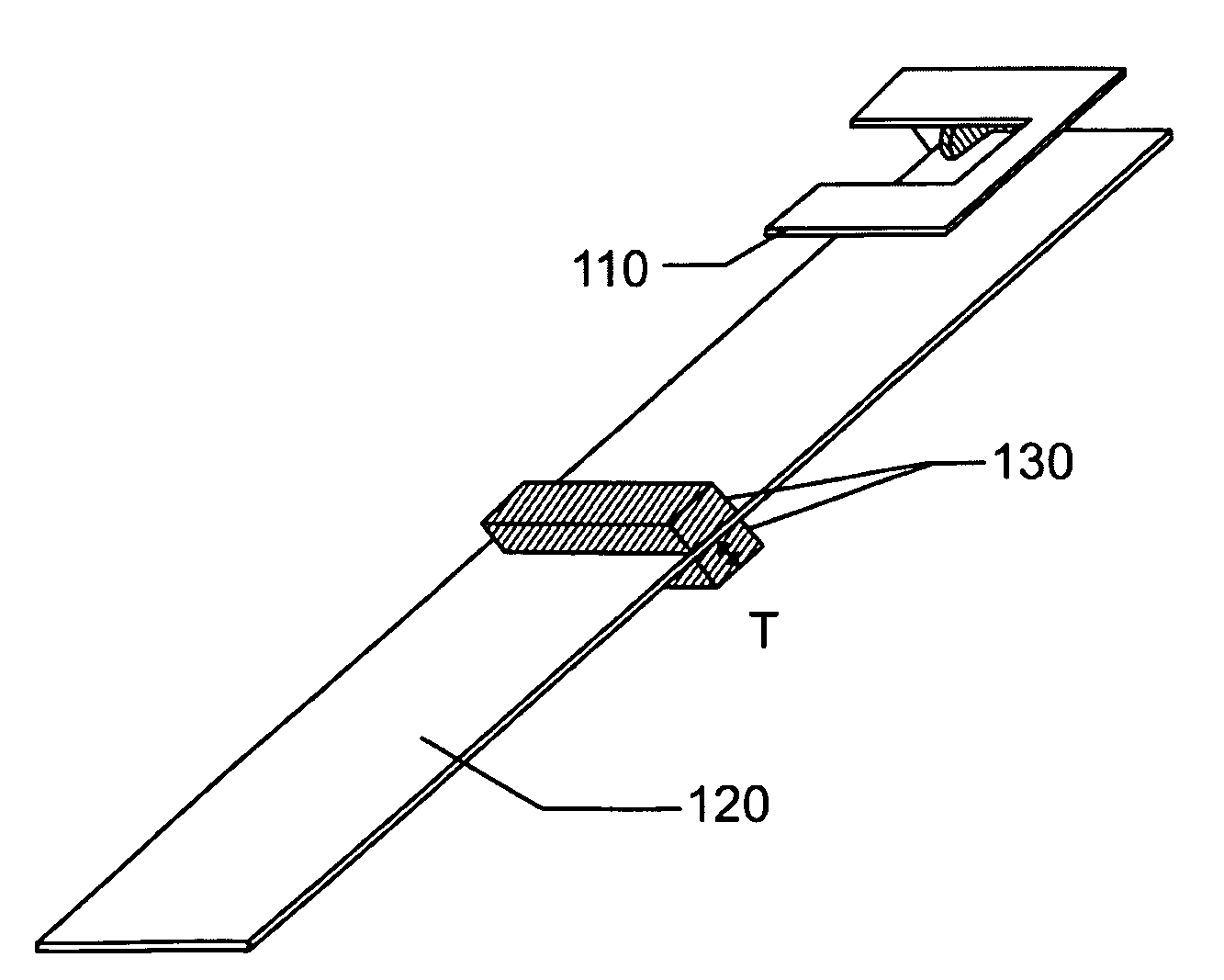
[0087]FIG. 14 shows a schematic exploded view of a portable electronic device comprising an antenna arrangement or adaptive system according to one of the embodiments. The portable electronic device such as e.g. a mobile phone can comprise a back cover 1410 and a front cover 1420, which in their assembled state form a housing of the portable electronic device. Furthermore, a PCB or PWB 1430 may be inserted into the housing in the assembled state where the front cover 1420 is fixed onto the back cover 1410. The PCB or PWB 1430 can comprise circuitry 1440 such as e.g. the circuitry described in connection with the Further, the PCB or PWB 1430 is shown with a schematic keypad and display and may correspond to the at least one ground plane element 120. That is, the portable electronic device as shown in FIG. 14 can comprise an antenna arrangement or adaptive system as described above.

[0088]The at least one magnetic element 130 may be integrated to the back cover 1410 and / or the front c...


PUM

PropertyMeasurementUnit
lengthaaaaaaaaaa
sizeaaaaaaaaaa
sizeaaaaaaaaaa

Abstract

The present invention relates to an antenna arrangement, an adaptive system comprising such arrangement, a portable electronic device comprising such arrangement or adaptive system, a method of manufacturing such an arrangement, and a computer-readable storage medium encoded with instructions for performing such method. The antenna arrangement can comprise at least one antenna element (110) configured to supply a current, at least one ground plane element (120) configured to conduct the current, and at least one magnetic element (130) configured to influence at least a part of the current in order to modify an electrical length of the at least one ground plane element (120). It enables to increase the electrical length of a terminal chassis, which may increase the operation bandwidth of the antenna-chassis combination. This effect can be further increased when combining at least one slot and at least one magnetic element covering the same at least partially.

Description

FIELD OF THE INVENTION[0001]The present invention relates to an antenna arrangement and a method of manufacturing such an antenna arrangement.BACKGROUND OF THE INVENTION[0002]Impedance bandwidth and total efficiency of small unbalanced antennas used in today's portable electronic devices such as mobile phones, mobile terminals and the like depend strongly on the largest dimension (typically length) of a metal and / or conductive structure that acts as a ground plane for an antenna. Typically, this ground plane, which is often called metal chassis of a terminal, can be formed by ground layers of a printed circuit board (PCB) or printed wiring board (PWB) and / or other metal objects attached to the same, such as radio frequency (RF) shields.[0003]However, when the length of the chassis is decreased below a certain size, e.g. 100 mm, it becomes difficult to design compact (internal) antennas that have sufficient impedance match and hence sufficiently large total efficiency to cover desire...

Claims


Application Information

Patent Timeline
Patent Type & Authority Applications(United States)
IPC IPC(8): H01Q1/24H01Q1/48H01P11/00H01Q1/00
CPCH01Q1/243Y10T29/49016H01Q1/48
Inventor OLLIKAINEN, JANI PETRI JUHANIZHAO, AN-PINGRAHOLA, JUSSI OLAVI
Owner NOKIA CORP
Why Eureka
Try Eureka