Solid-state imaging device

a solid-state imaging and imaging device technology, applied in the direction of radioation control devices, television system scanning details, television systems, etc., can solve problems such as possible residual image electrons

Active Publication Date: 2009-12-31
PANASONIC SEMICON SOLUTIONS CO LTD
View PDF25 Cites 21 Cited by
  • Summary
  • Abstract
  • Description
  • Claims
  • Application Information

AI Technical Summary

Benefits of technology

[0031]In the reset signal RST high level period between t1 to t2b shown in FIGS. 11A and 11B, however, the reset transistor 136 in FIG. 8 turns on, and the level of voltage of the floating diffusion (FD) 138 is fixed to the FD reset potential 1. Thus no coupling effect of C102 is obtained. An actual period in which the coupling effect of the C102 is available is a period that the reset signal RST becomes a low level and that the floating diffusion (FD) 138 is in a floating state by turning the reset transistor 136 off, as well as a period in which the level of voltage of the column signal line 153 rises by the output from the amplifying transistor 142. Thus, t2b to t2 in FIGS. 11A and 11B is the only period that the coupling effect of the C102 is available.

Problems solved by technology

Since the period is short in obtaining the coupling effect of the C102, increase in FD capacitance caused by a rise in FD reset level of voltage may be limited, causing possible residual image electrons.

Method used


Image

  • Solid-state imaging device
  • Solid-state imaging device
  • Solid-state imaging device

Examples


embodiment

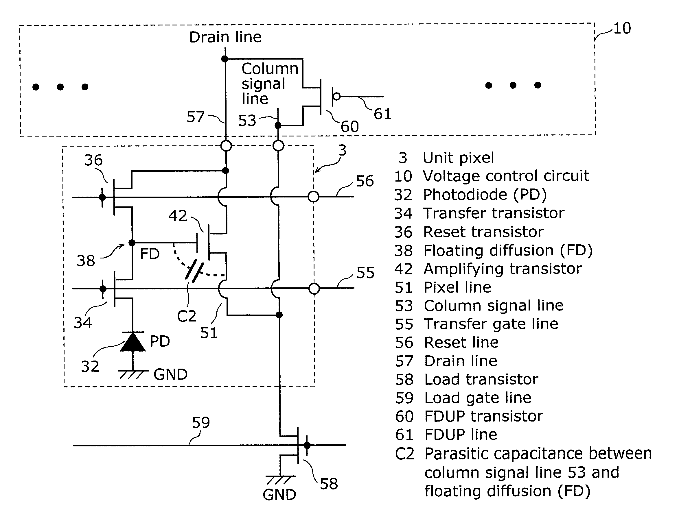
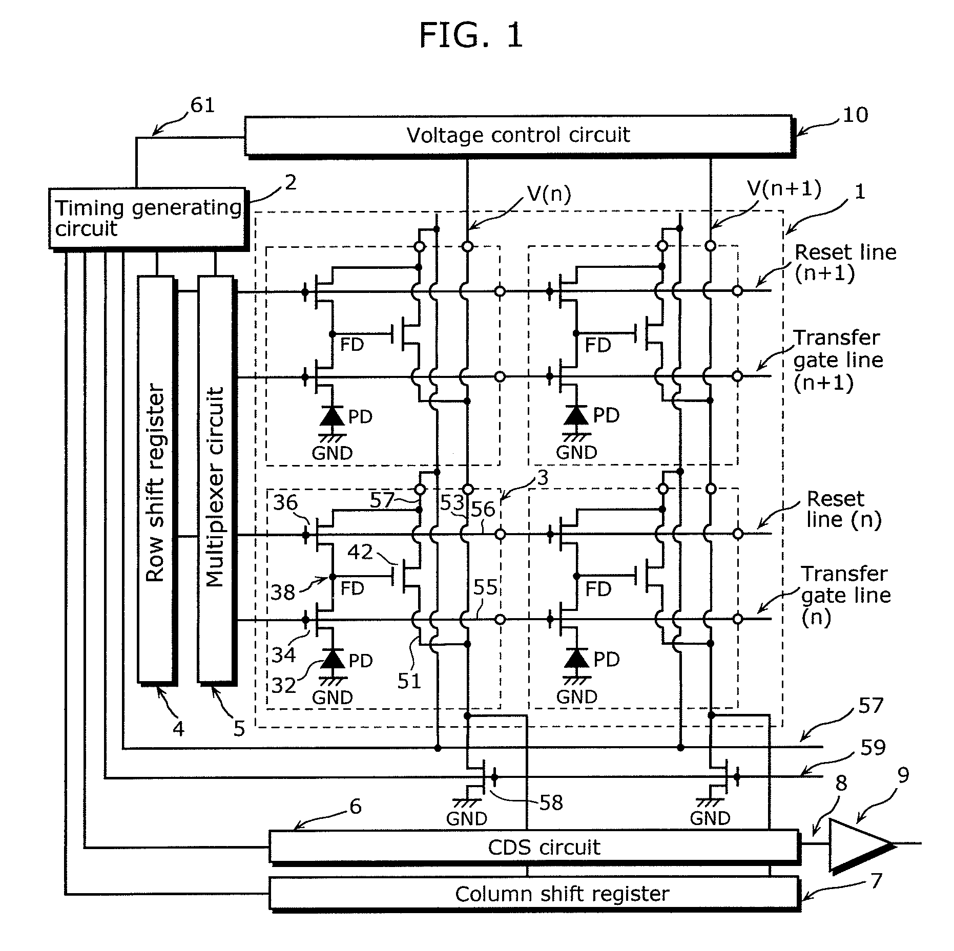
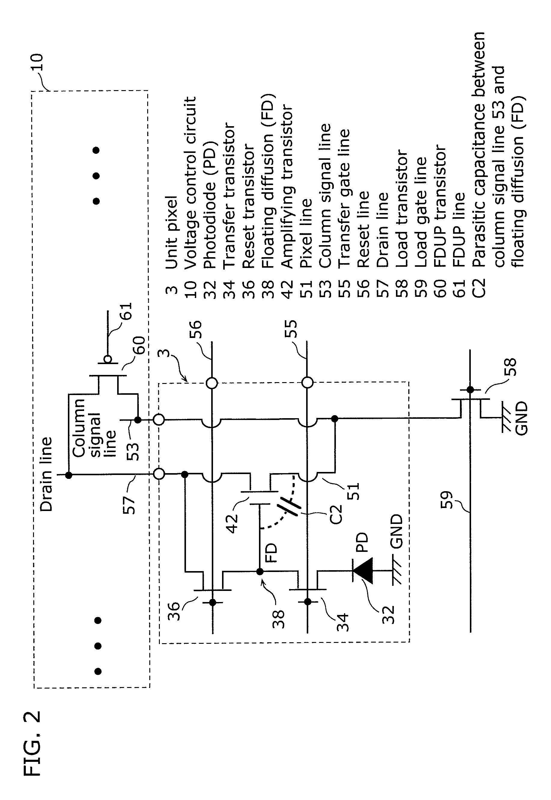
[0066]FIG. 1 is a block diagram showing a structure of a solid-state imaging device in embodiment of the present invention.

[0067]The solid-state imaging device in FIG. 1 includes plural unit pixels 3, column signal lines 53, a timing generating circuit 2, a row shift register 4, a multiplexer circuit 5, a Correlated Double Sampling (CDS) circuit 6, a column shift register 7, a row signal line 8, an output amplifier 9, and a voltage control circuit 10. Here, each of the column signal lines 53 is connected to associated amplifying transistors corresponding to an associated column of the corresponding unit pixels 3.

[0068]The column signal line 53 is connected to the associated column of the corresponding unit pixels 3, and provides to the CDS circuit 6 a is signal forwarded from the associated unit pixel 3. Here, the connected column signal line 53 and each of unit pixels 3 are arranged on the same column. The column signal lines connected to pixels on the nth column and the n+1th colu...

modification 1

of Embodiment

[0117]Described next is Modification 1 of the embodiment in the present invention.

[0118]A solid-state imaging device in the modification includes the gate of the FDUP transistor 60 connected to a bias line having a voltage higher than that of the drain line 57.

[0119]Mainly described hereinafter are points different from embodiment of the present invention.

[0120]FIG. 5 is a circuit diagram showing a structure of a unit pixel and a circuit surrounding the unit pixel in the modification.

[0121]The source of the FDUP transistor 60 in the modification is connected to a bias line 62 having a voltage higher than that of the drain line 57 in order to bring high the level of voltage of the column signal line 53. For example, the bias line 62 has a bias voltage; that is, a voltage of the drain line 57 boosted by a charge pump circuit.

[0122]Since this allows the solid-state imaging device of the modification to further increase a rising amplitude of the column signal line 53, the c...

modification 2

of Embodiment

[0123]Described next is Modification 2 of embodiment in the present invention.

[0124]A solid-state imaging device in the modification includes a cell having plural unit pixels each including one photodiode and one transfer transistor. Chiefly described hereinafter are points different from embodiment of the present invention.

[0125]FIG. 6 shows a structure of a cell and a circuit surrounding the cell in the modification. The solid-state imaging device in the modification includes a cell 70 each having four unit pixels. Here, each unit pixel has one of photodiodes 32a (PDa) to 32d (PDd) and one of transfer transistors 34a to 34b.

[0126]Instead of the PD 32 and the transfer transistor 34 in embodiment, the cell 70 includes the plural photodiodes 32a (PDa) to 32d (PDd) and the plural transfer transistors 34a to 34d.

[0127]Each of the photodiodes 32a (PDa) to 32d (PDd) generates a signal charge corresponding to an incident electromagnetic wave. One end of the photodiode is co...


PUM


Abstract

A solid-state imaging device includes: plural pixel cells, arranged in a matrix, each of which includes a photodiode which photoelectrically converts incident light, a transferring transistor which transfers a charge generated by the photodiode, a floating diffusion which accumulates the transferred charge, a reset transistor which resets a potential of said floating diffusion, and an amplifying transistor which converts the charge accumulated in the floating lo diffusion into a voltage; column signal lines each connected to associated ones of plurality of amplifying transistors including the amplifying transistor corresponding to a corresponding one of columns having the associated plurality of pixel cells; and a voltage control circuit which increases a voltage of the column signal line to a predetermined voltage between the reset of the potential by the reset transistor and the transfer of the charge by the transferring transistor.

Description

BACKGROUND OF THE INVENTION[0001](1) Field of the Invention[0002]The present invention relates to a solid-state imaging device including plural pixel cells arranged in a matrix, and a column signal lines connected to plural amplifying transistors corresponding to a column of the associated plural pixel cells.[0003](2) Description of the Related Arts[0004]Recently, manufacturers are promoting developments of MOS solid-state image sensors as solid-state imaging devices applicable to video cameras and electronic still cameras. These solid-state imaging devices are structured to amplify, using a MOS transistor, a signal obtained by a photoelectric conversion unit on a cell basis, and pick up the amplified signal.[0005]FIG. 8 is a circuit diagram illustrating a unit pixel included in a conventional solid-state imaging device having a MOS transistor and a circuit surrounding the unit pixel.[0006]A unit pixel 103 included in a MOS image sensor has a photodiode (PD) 132, a transfer transist...

Claims


Application Information

Patent Timeline
Patent Type & Authority Applications(United States)
IPC IPC(8): H04N5/335H01L27/146H04N5/357H04N5/369H04N5/372H04N5/374
CPCH01L27/14643H04N5/3559H01L27/14641H04N5/37457H04N5/359H04N25/59H04N25/62H04N25/778
Inventor ISHIMOTO, HISATOMURAKAMI, MASASHI
Owner PANASONIC SEMICON SOLUTIONS CO LTD
Why Eureka
Try Eureka