Semiconductor device or printed wiring board design method and design support system that implements settings by using a semiconductor device model that expresses parasitic elements that occur when packaged

a technology of semiconductor devices and support systems, applied in the direction of detecting faulty computer hardware, instruments, error detection/correction, etc., can solve the problems of parasitic elements that occur between the semiconductor chip and the semiconductor package, the design time becomes long, and the design of a device that includes an already designed semiconductor chip is difficult to apply to the design of a device that includes an already designed semiconductor chip

Inactive Publication Date: 2009-12-31
ELPIDA MEMORY INC
View PDF4 Cites 11 Cited by
  • Summary
  • Abstract
  • Description
  • Claims
  • Application Information

AI Technical Summary

Problems solved by technology

Because voltage fluctuation is analyzed each time a layout is corrected in transient analysis, the problem arises that the design time becomes lengthy as the number of layout corrections increase.
However, the technique of Patent Document 2 takes as its object the layout on a semiconductor chip, and the technique described in Patent Document 2 is therefore difficult to apply to the design of a device that includes an already designed semiconductor chip.
It was therefore impossible to model parasitic elements that occur between the semiconductor chip and the semiconductor package or parasitic elements that occur betw

Method used


Image

  • Semiconductor device or printed wiring board design method and design support system that implements settings by using a semiconductor device model that expresses parasitic elements that occur when packaged
  • Semiconductor device or printed wiring board design method and design support system that implements settings by using a semiconductor device model that expresses parasitic elements that occur when packaged
  • Semiconductor device or printed wiring board design method and design support system that implements settings by using a semiconductor device model that expresses parasitic elements that occur when packaged

Examples


Embodiment Construction

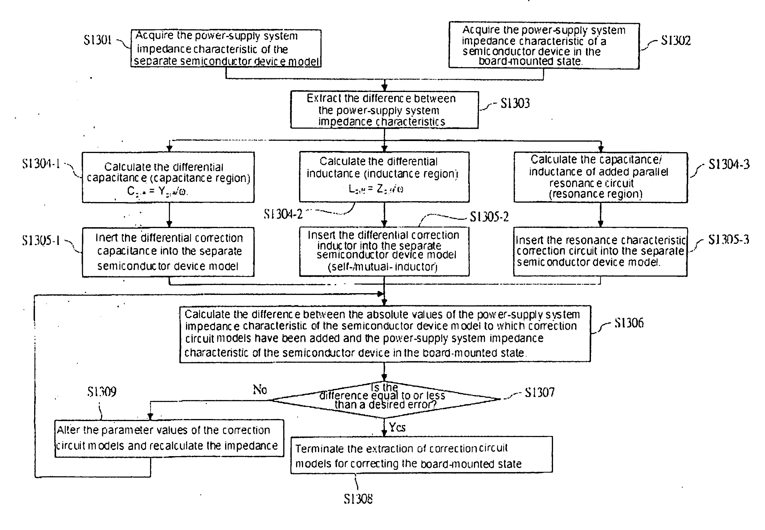
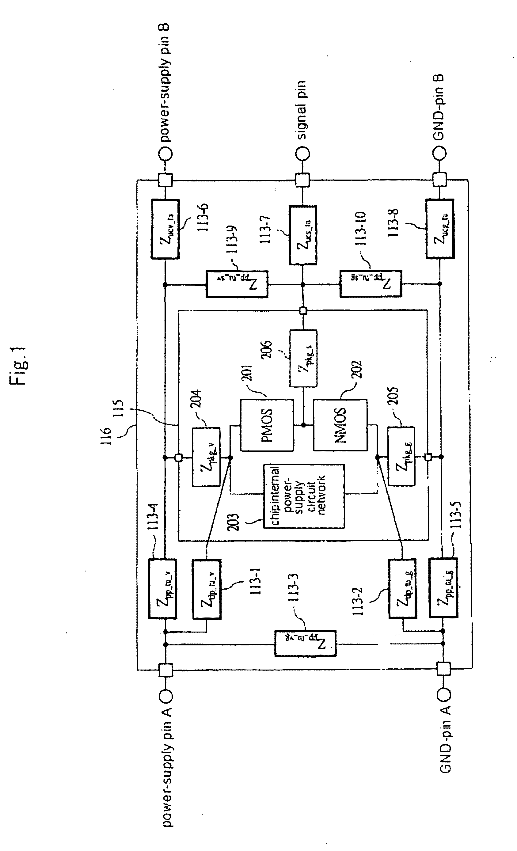
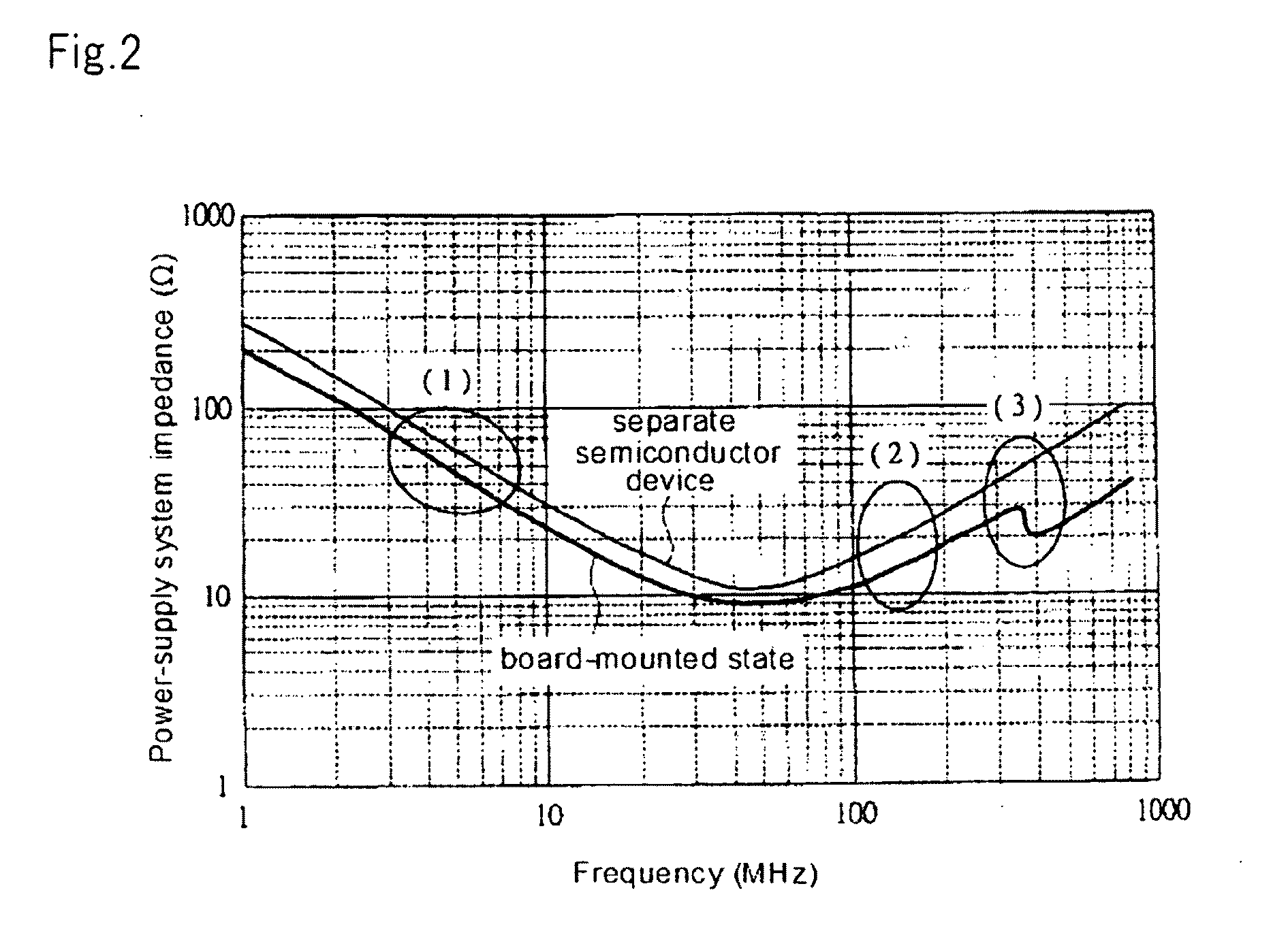
[0036]Before describing of the present invention, the prior art will be explained in detail in order to facilitate the understanding of the present invention When a semiconductor device is mounted on a printed wiring board, parasitic elements are produced in at least one of the semiconductor device and printed wiring board. The semiconductor device includes a semiconductor chip or a semiconductor package in which a semiconductor chip is mounted.

[0037]In addition, examples of the above-described parasitic elements include, for example, parasitic capacitance that occurs between the printed wiring board and the semiconductor chip and / or semiconductor package, and mutual inductance or parasitic inductance that occurs between the semiconductor package and printed wiring board.

[0038]Examples of parasitic capacitance that is produced between the printed wiring board and the semiconductor chip and / or the semiconductor package include, for example, parasitic capacitance that is occurs betwee...


PUM


Abstract

Correction circuit models are acquired for correcting electrical characteristic parameters that change upon mounting on a board. The correction circuit models are added to a separate model that represents a separate semiconductor device in isolation to create a semiconductor device model that represents the semiconductor device in a board-mounted state. An equivalent circuit model that represents an adjustment-object system is connected to the semiconductor device model that was created, and based on the semiconductor device model to which the equivalent circuit model is connected, adjustment-object values relating to the adjustment-object system are calculated. These adjustment-object values are compared with limit values that were determined in advance, and based on the results of comparison, a design guide is determined for adjusting the adjustment-object system.

Description

BACKGROUND OF THE INVENTION[0001]1. Field of the Invention[0002]The present invention relates to a design method and a design support system of a semiconductor device or a printed wiring board.[0003]2. Description of the Related Art[0004]In a device having a semiconductor chip, a design is necessary that keeps voltage fluctuation in the power-supply pad and / or ground pad to no greater than a permissible value. As a result, in the design stage of a device that includes a semiconductor chip, the suitability of the design of the device that includes the semiconductor chip is determined by analyzing the voltage fluctuation in the power-supply pad and / or ground pad of the semiconductor chip. Examples of a device that includes a semiconductor chip include, for example, a semiconductor package, a printed wiring board on which a semiconductor package is mounted, and any device that includes a printed wiring board on which a semiconductor package is mounted.[0005]As an example of the above-d...

Claims


Application Information

Patent Timeline
IPC IPC(8): G06F17/50
CPCG06F17/5036H05K3/0005H05K1/181G06F2217/78G06F30/367G06F2119/06
Inventor NAKAMURA, SATOSHIHARA, TSUTOMUKATAGIRI, MITSUAKIHIROSE, YUKITOSHIITAYA, SATOSHIIWAKURA, KEN
Owner ELPIDA MEMORY INC
Why Eureka
Try Eureka