Electrophoretic display device and electronic apparatus
- Summary
- Abstract
- Description
- Claims
- Application Information
AI Technical Summary
Benefits of technology
Problems solved by technology
Method used
Image
Examples
first embodiment
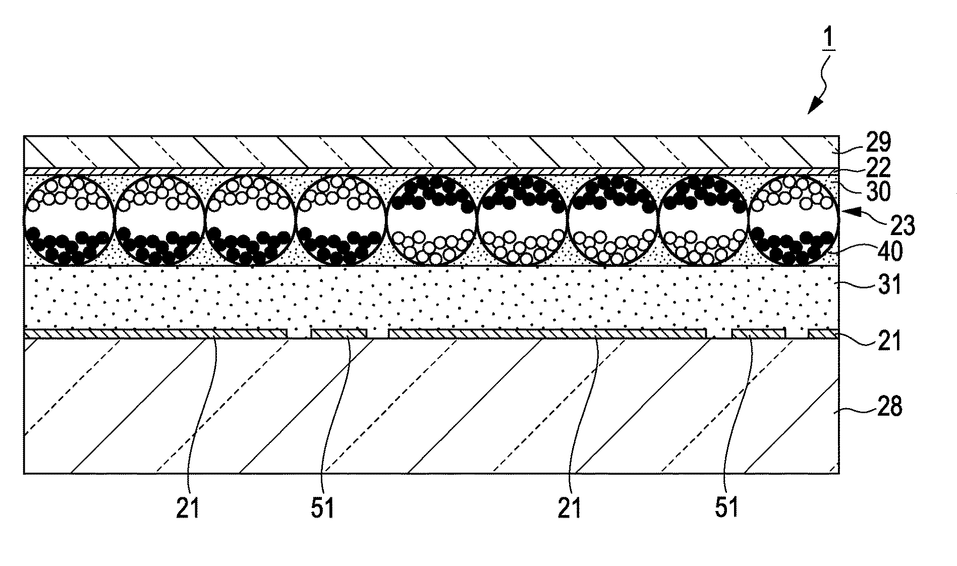
[0037]Hereinafter, an electrophoretic display device according to a first embodiment of the invention will be described with reference to FIGS. 1A to 5C. In all the drawings described below, for easy understanding of the drawings, the scales of the film thicknesses and dimensions of constituent elements are differently set appropriately.
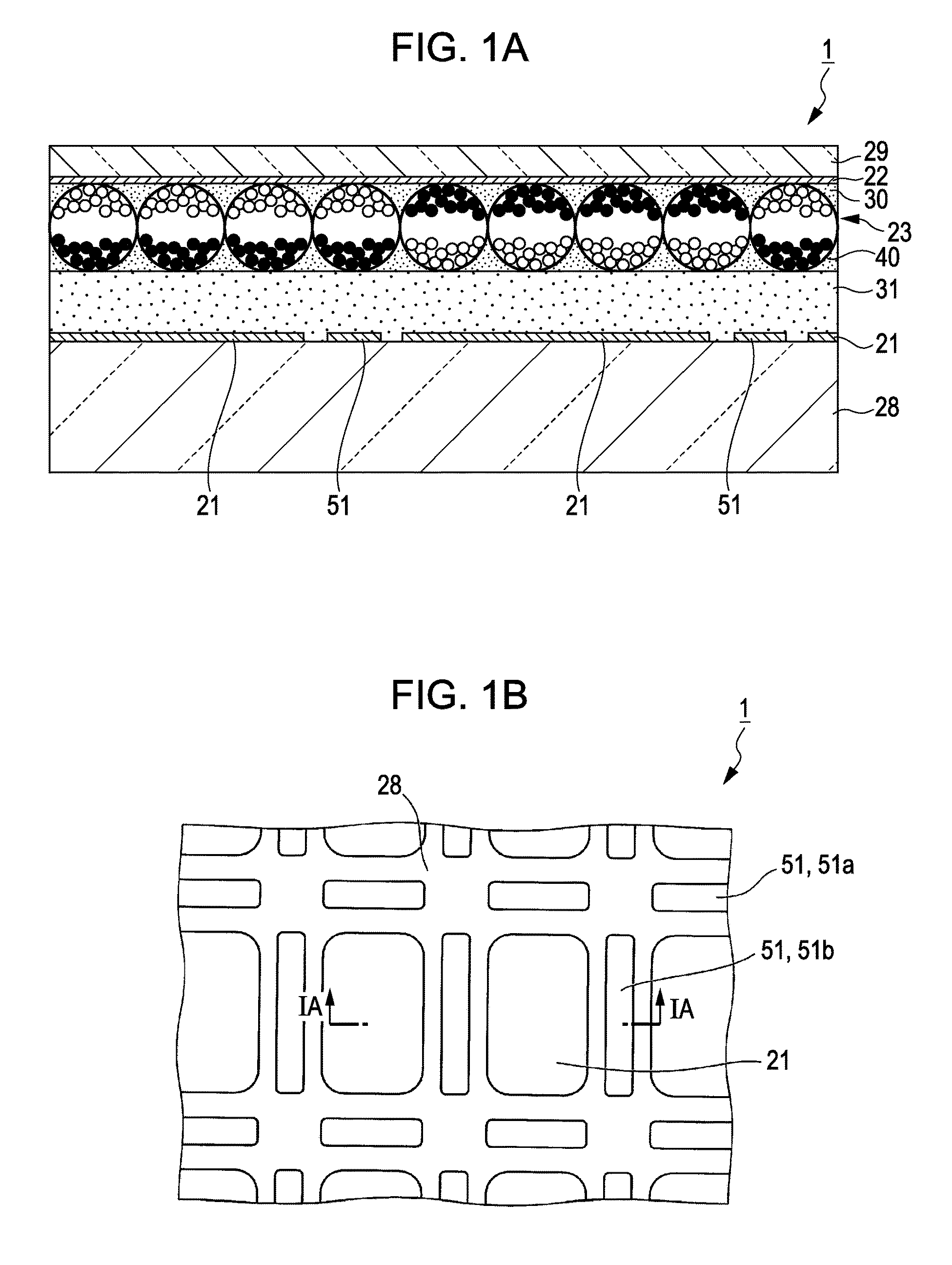
[0038]FIGS. 1A and 1B are explanatory diagrams of an electrophoretic display device 1 according to this embodiment. FIG. 1A is a cross-section view of the electrophoretic display device 1, and FIG. 1B is a plan view of the electrophoretic display device 1. FIG. 1A is a cross-section view taken along line IA-IA shown in FIG. 1B.
[0039]As shown in FIG. 1A, the electrophoretic display device 1 according to this embodiment includes a component substrate (first substrate) 28 that has a plurality of pixel electrodes 21, an opposing substrate (second substrate) 29 that has a common electrode 22, and an electrophoretic element layer 23 that is sandwiched by b...
modified examples
[0075]Based on the purpose of the invention of suppressing the leakage current by disposing the intermediate electric potential electrode between adjacent pixel electrodes so as to change the propagation pattern of the electric field (lines of electric force), it is apparent that the shape or the disposition of the intermediate electric potential electrode can be changed. Hereinafter, the shape and the disposition of the intermediate electric potential electrode according to several modified examples will be described. FIGS. 5A to 5C are plan views of the modified examples and are diagrams corresponding to FIG. 1B.
[0076]In FIG. 5A, the intermediate electric potential electrodes 52a extend up to intersections of pixel electrodes 21 that are disposed vertically and horizontally in a lattice shape in the plan view. In other words, the intermediate electric potential electrode 52a that is disposed along the short side of the pixel electrode 21 extends along an extended line of the short...
second embodiment
[0080]FIGS. 6A and 6B are explanatory diagrams of an electrophoretic display device according to a second embodiment of the invention. FIG. 6A is a cross-section view of the electrophoretic display device, and FIG. 6B is a plan view of electrophoretic display device. FIG. 6A shows a cross-section view taken along line VIA-VIA shown in FIG. 6B.
[0081]The electrophoretic display device according to this embodiment is common to a part of that according to the first embodiment. A difference between the first embodiment and the second embodiment is that an insulation layer 60 that covers the intermediate electric potential electrodes 51 and protrudes to the electrophoretic element layer 23 side relative to upper faces of the pixel electrodes 21 is formed in the second embodiment. Thus, to each constituent element of the second embodiment that is common to the first embodiment, a same reference sign is assigned, and a detailed description thereof is omitted here.
[0082]As shown in FIG. 6A, ...
PUM
 Abstract
Description
Claims
Application Information


