

Semiconductor device
- Summary
- Abstract
- Description
- Claims
- Application Information
AI Technical Summary
Benefits of technology
Problems solved by technology
Method used
Image

Examples
first embodiment
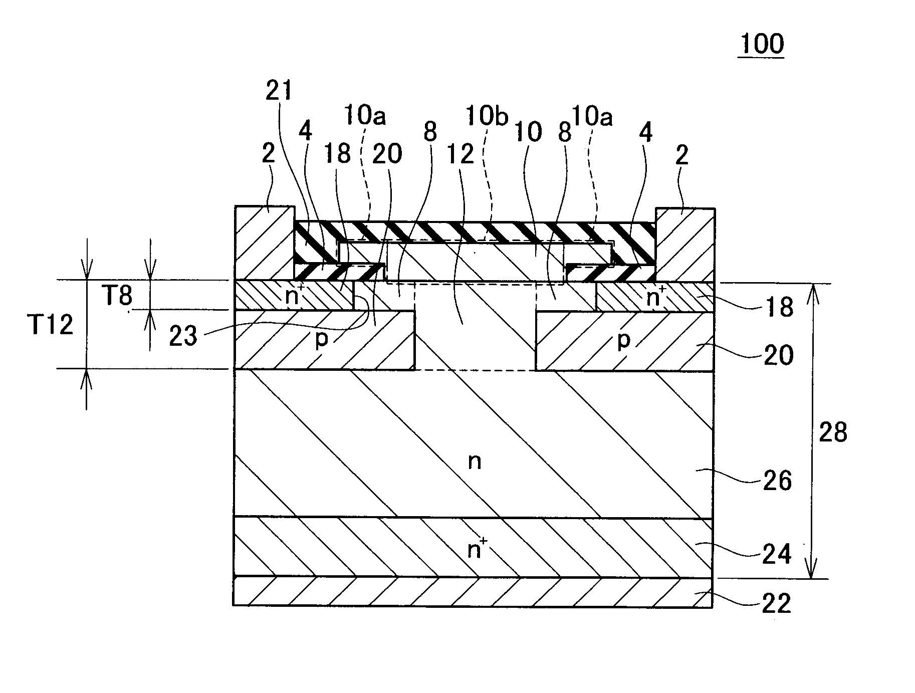
[0030]A semiconductor device of a first embodiment will be described. FIG. 1 shows a cross-sectional view of essential parts of a vertical semiconductor device 100. The semiconductor device 100 is a vertical transistor having a pair of source electrodes 2 disposed on a surface of a semiconductor substrate 28, and a drain electrode 22 disposed on a rear surface of the semiconductor substrate 28. A gate electrode 10 is disposed between the pair of source electrodes 2 and the drain electrode 22. Actually, the gate electrode 10 is located between the drain electrode 22 and each of the source electrode 2. The gate electrode 10 switches the state of electric current between the drain electrode 22 and the pair of source electrodes 2 between a conducting state and a non-conducting state. Although this will be described later, the gate electrode 10 (which is an example of the gate structure) has an insulating gate part 10a and a Schottky gate part 10b. The semiconductor device 100 is utilize...
second embodiment
[0045]A semiconductor device of a second embodiment will now be described. FIG. 8 shows a cross-sectional view of essential parts of a semiconductor device 200. The semiconductor device 200 is a variant of the semiconductor device 100. The semiconductor device 200 is a lateral type transistor. A channel region 208 and a drift region 212 are disposed on a surface of a p-type semiconductor region 220. Thickness T208 of the channel region 208 is thinner than thickness T212 of the drift region 212. As a result, when voltage is not being applied to a gate electrode 210, the channel region 208 is depleted by a depletion layer extending from the p-type semiconductor region 220. As a result, electrons cannot move from a source region 218 to the drift region 212.
[0046]As in the case of the semiconductor device 100, in the semiconductor device 200, the gate electrode 210 has an insulating gate part 210a and a Schottky gate part 210b. The insulating gate part 210a is disposed on a portion of a...
third embodiment
[0047]A semiconductor device of a third embodiment will now be described. FIG. 9 shows a cross-sectional view of essential parts of a semiconductor device 300. The semiconductor device 300 is a variant of the semiconductor device 200. The semiconductor device 300 is also a lateral type transistor. Different from the semiconductor device 200, in the semiconductor device 300, thickness of a semiconductor substrate 328 is uniform. Furthermore, in the semiconductor device 300, thickness of a p-type semiconductor region 320 varies. The p-type semiconductor region 320 is thick in a range 328a, and is thin in a range 328b. As a result, thickness T312 of a drift region 312 is thicker than thickness T308 of a channel region 308. Since the thickness of the p-type semiconductor region 320 is varied in the semiconductor device 300, the thickness T312 of the drift region 312 can be made thicker than the thickness T308 of the channel region 308, while the thickness of the semiconductor substrate ...
PUM
 Abstract
Description
Claims
Application Information