Transistor and semiconductor device

a technology of semiconductor devices and transistors, applied in the direction of semiconductor devices, electrical equipment, basic electric elements, etc., can solve the problems of reducing the mobility of the entire transistor. , to achieve the effect of controlling large current, increasing the resistance of the channel formation region in the vicinity of the drain, and reducing the mobility of the entire transistor

Active Publication Date: 2012-08-02
SEMICON ENERGY LAB CO LTD
View PDF5 Cites 44 Cited by
  • Summary
  • Abstract
  • Description
  • Claims
  • Application Information

AI Technical Summary

Benefits of technology

[0022]When the capacitance of the gate insulating layer in the vicinity of the first electrode functioning as a drain electrode is made smaller, the resistance of the channel formation region in the vicinity of the drain is increased. Accordingly, an electric field generated in the oxide semiconductor layer in the vicinity of the drain is reduced, so that a transistor which withstands a high voltage and does not breakdown even when a high electric field is applied to the drain electrode.
[0023]In addition, when the capacitance of the gate insulating layer except the vicinity of the drain is made larger as compared to the capacitance of the gate insulating layer in the vicinity of the drain, a reduction in the mobility of the entire transistor can be prevented, so that control of large current is possible and a semiconductor device with high resistance can be provided.

Problems solved by technology

By a series of processes, current of the transistor is intensively increased and heat due to Joule heat is generated locally, which leads to breakdown of the transistor.
When a high electric field of 3 MV / cm or more is applied to a transistor including silicon carbide, the transistor breaks down and loses a function of a transistor in some cases.

Method used


Image

  • Transistor and semiconductor device
  • Transistor and semiconductor device
  • Transistor and semiconductor device

Examples


embodiment 1

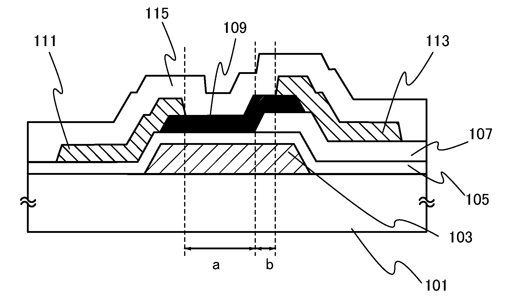
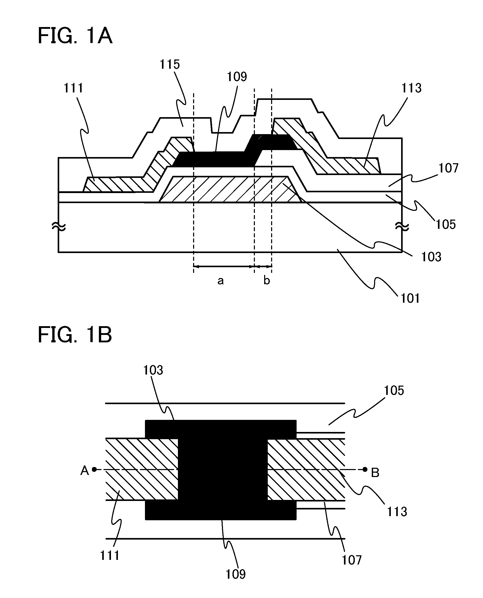
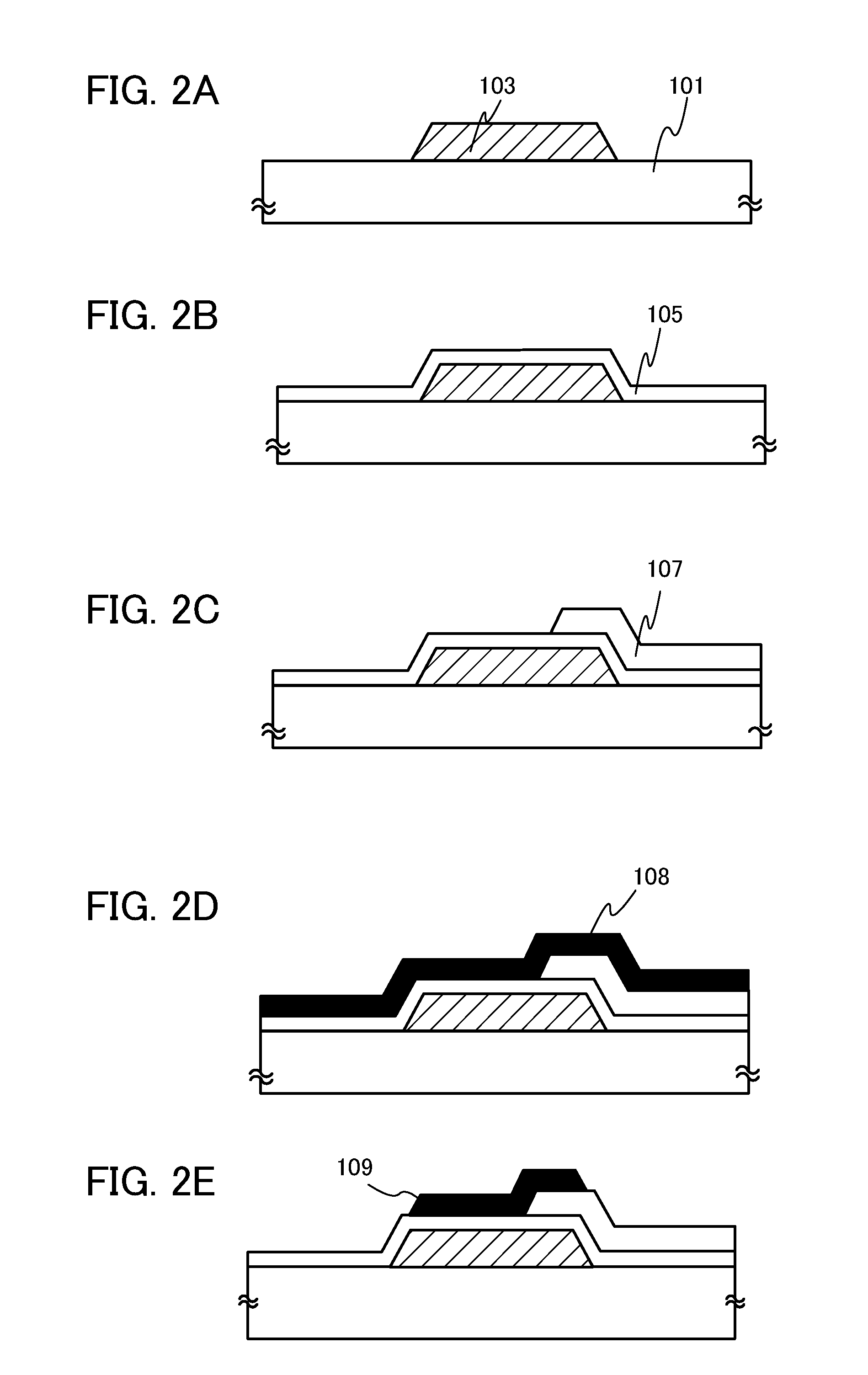
[0068]In this embodiment, examples of the structure of a transistor according to one embodiment of the present invention and a method for manufacturing the transistor will be described with reference to FIGS. 1A and 1B, FIGS. 2A to 2E, FIGS. 3A to 3D, and FIGS. 11A and 11B. Note that a first electrode and a second electrode of a transistor are referred to as a drain electrode and a source electrode, respectively in this embodiment.

[0069]FIGS. 1A and 1B illustrate the structure of a transistor according to one embodiment of the present invention. FIG. 1B is a top view of the transistor according to one embodiment of the present invention, and FIG. 1A is a cross-sectional view taken alone line A-B of the transistor illustrated in FIG. 1B. The transistor illustrated in FIGS. 1A and 1B has a structure in which a second gate insulating layer stacked in the vicinity of a drain is included in addition to a first gate insulating layer, and the thickness of a gate insulating layer is partial...

embodiment 2

[0181]In this embodiment, transistors according to one embodiment of the present invention which are different from those of Embodiment 1 will be described. FIGS. 4A and 4B each illustrate a transistor of this embodiment. Note that a first electrode and a second electrode of a transistor are referred to as a drain electrode and a source electrode, respectively in this embodiment.

[0182]A transistor of one embodiment of the present invention includes, as illustrated in FIG. 4A, a substrate 401; an island-shaped first gate electrode 403 provided over the substrate 401; a first gate insulating layer 405 provided to cover the first gate electrode 403; an oxide semiconductor layer 407 which is provided over the first gate insulating layer 405 to overlap with the first gate electrode 403 and whose length in a channel length direction is longer than that of the first gate electrode 403; a pair of a source electrode 409 and a drain electrode 411 whose end portions overlap with the oxide semi...

embodiment 3

[0201]In this embodiment, examples of a semiconductor device using the transistor described the above embodiment will be described. For example, a circuit which converts DC voltage at a given value into DC voltage at another value (also referred to as a DC converter circuit or a DC-DC converter) can be used in the case where power supply voltage at a stable value is generated from voltage with large fluctuation or in the case where power supply voltage at a plurality of different values is needed. The transistor described in the above embodiment is a transistor with improved withstand voltage; therefore, a highly reliable DC converter circuit can be formed using the transistor.

[0202]Further, the DC converter circuit in which the transistor is used can form a power supply circuit by combining with a variety of power storage devices. In this embodiment, a power supply circuit including the transistor described in the above embodiment will be described.

[0203]An example of a configurati...


PUM


Abstract

A transistor which withstands a high voltage and controls large electric power can be provided. A transistor is provided which includes a gate electrode, a gate insulating layer over the gate electrode, an oxide semiconductor layer which is over the gate insulating layer and overlaps with the gate electrode, and a source electrode and a drain electrode which are in contact with the oxide semiconductor layer and whose end portions overlap with the gate electrode. The gate insulating layer includes a first region overlapping with the end portion of the drain electrode and a second region adjacent to the first region. The first region has smaller capacitance than the second region.

Description

BACKGROUND OF THE INVENTION[0001]1. Field of the Invention[0002]The present invention also relates to a semiconductor device including an oxide semiconductor.[0003]In this specification, a “semiconductor device” refers to all devices which can function by utilizing semiconductor characteristics, and electro-optical devices, semiconductor circuits, electronic components, and electronic devices are all included in the category of the semiconductor device.[0004]2. Description of the Related Art[0005]In a semiconductor device with high withstand voltage for controlling large current, a so-called power device, silicon has been used mainly as a semiconductor material. However, it is said that the physical characteristics of a transistor using silicon reach the theoretical value limit, and a novel semiconductor material with which the characteristics can be improved has been demanded in order to realize a power device that has high withstand voltage and can control large current. As the se...

Claims


Application Information

Patent Timeline
Patent Type & Authority Applications(United States)
IPC IPC(8): H01L29/78
CPCH01L29/7869H01L29/42384H01L29/78648
Inventor GODO, HIROMICHIKOBAYASHI, SATOSHITSUBUKU, MASASHI
Owner SEMICON ENERGY LAB CO LTD
Why Eureka
Try Eureka