Thin film transistor substrate and method for manufacturing the same

a technology of thin film transistors and substrates, applied in the direction of instruments, semiconductor devices, electrical equipment, etc., can solve the problems of alignment errors, assembly errors, alignment errors, etc., and achieve the effect of reducing the length of the contact hole and being easy to execu

Active Publication Date: 2010-01-28
SAMSUNG DISPLAY CO LTD
View PDF18 Cites 11 Cited by
  • Summary
  • Abstract
  • Description
  • Claims
  • Application Information

AI Technical Summary

Benefits of technology

[0027]In one exemplary embodiment, the height increasing member may be disposed in a region totally overlapped by the drain electrode. According to an exemplary embodiment of the present invention, the height increasing member is formed under the contact hole for the contact between the pixel electrode and the thin film transistor such that the length of the contact hole is reduced, thereby easily executing the dry-etching process for the forming of the contact hole.

Problems solved by technology

However, in the abovedescribed LCD, the pixel electrodes and the color filters are disposed on different display panels such that it is difficult to align the pixel electrodes and the color filters to each other, thereby generating an alignment error.
However the process is not easy and may lead to assembly errors and increased manufacturing costs.

Method used


Image

  • Thin film transistor substrate and method for manufacturing the same
  • Thin film transistor substrate and method for manufacturing the same
  • Thin film transistor substrate and method for manufacturing the same

Examples


first exemplary embodiment

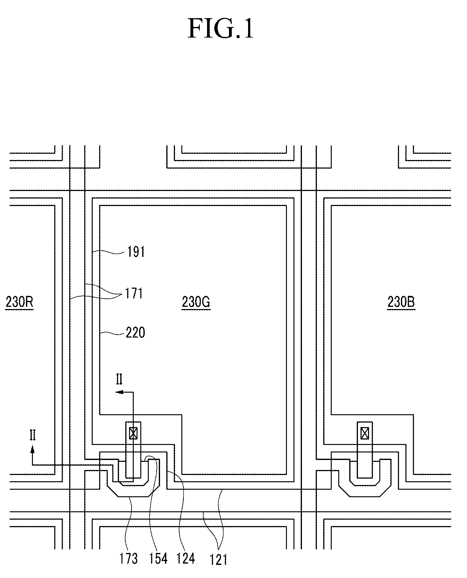
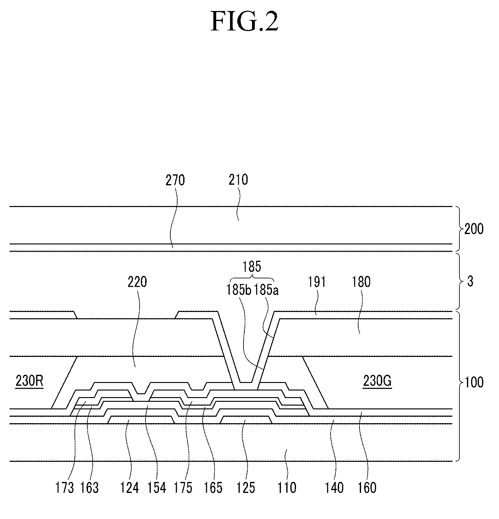
[0046]Now, a first exemplary embodiment of a liquid crystal display (“LCD”) according to the present invention will be described with reference to FIG. 1 and FIG. 2. FIG. 1 is a top plan layout view of the first exemplary embodiment of an LCD according to the present invention, and FIG. 2 is a cross-sectional view of the first exemplary embodiment of an LCD shown in FIG. 1 taken along line II-II.

[0047]Referring to FIG. 1 to FIG. 2, an LCD according to the present exemplary embodiment includes a thin film transistor (“TFT”) array panel 100 and a common electrode panel 200 facing each other, and a liquid crystal layer 3 interposed between two display panels 100 and 200. Firstly, the TFT array panel 100 will be described.

[0048]A plurality of gate lines 121 including gate electrodes 124, a height increasing member 125, a gate insulating layer 140, a plurality of semiconductors 154, a plurality of ohmic contacts 163 and 165, and a plurality of data lines 171 and a plurality of drain elec...

second exemplary embodiment

[0079]A second exemplary embodiment of an LCD according to the present invention will be described with reference to FIG. 12 to FIG. 15.

[0080]FIG. 12 is a top plan layout view of second exemplary embodiment of an LCD according to the present invention, FIG. 13 is a cross-sectional view of the second exemplary embodiment of an LCD shown in FIG. 12 taken along line XIII-XIII, and FIG. 14 is a cross-sectional view of the second exemplary embodiment of an LCD shown in FIG. 12 taken along line XIV-XIV.

[0081]As shown in FIG. 12 to FIG. 14, the second exemplary embodiment of an LCD according to the present invention is similar to the first exemplary embodiment of an LCD.

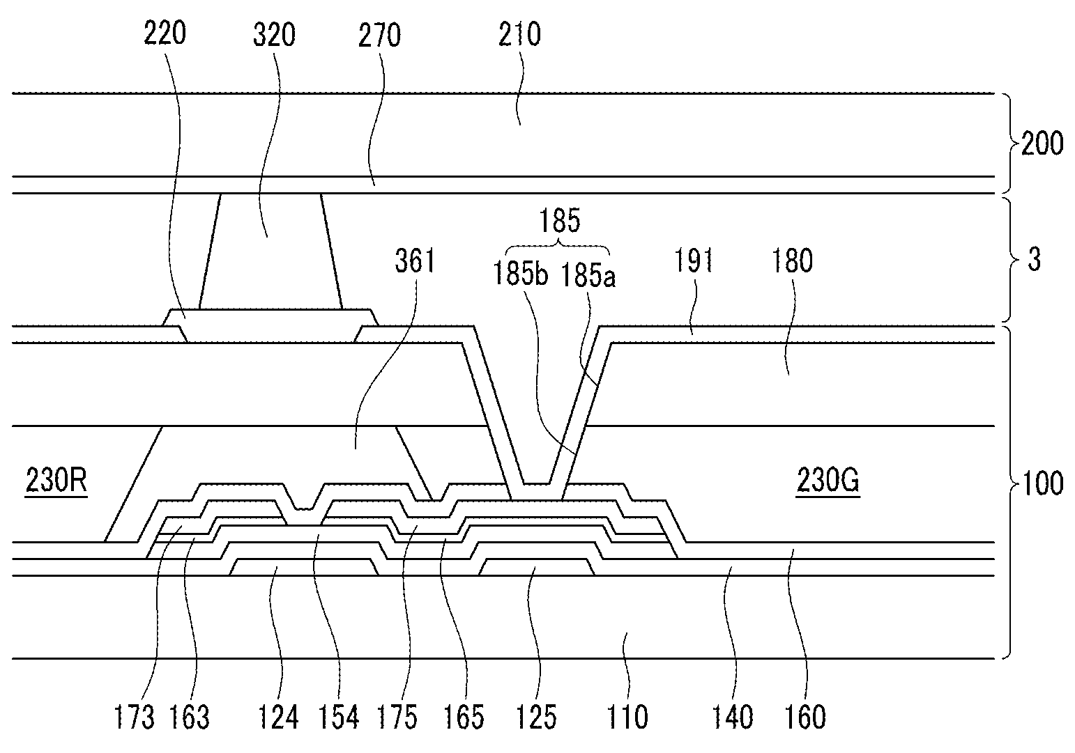
[0082]However, a partition 361 is formed on a portion corresponding to the gate line 121, the data line 171, and the TFT on the blocking layer 160, and the color filters 230R, 230G, and 230B are formed in the pixel area defined by the partition 361. This is different from the first exemplary embodiment in that the partition...


PUM


Abstract

A method for manufacturing a thin film transistor array panel includes; forming a gate line including a gate electrode and a height increasing member on a substrate, forming a gate insulating layer on the gate line and the height increasing member, forming a semiconductor, a data line including a source electrode, and a drain electrode facing the source electrode and overlapping at least a portion of the height increasing member on the gate insulating layer, forming a first insulating layer on the gate insulating layer, a data line and the drain electrode, forming a light-blocking member on a portion of the first insulating layer corresponding to the gate line and the data line, forming a color filter in an area bound by the light-blocking member, forming a second insulating layer on the light-blocking member and the color filter, and patterning the second insulating layer, the light-blocking member or the color filter, and the first insulating layer to form a contact hole exposing a portion of the drain electrode aligned with the height increasing member.

Description

[0001]This application claims priority to Korean Patent Application No. 10-2008-0072704, filed on Jul. 25, 2008, and all the benefits accruing therefrom under 35 U.S.C. §119, the contents of which in its entirety are herein incorporated by reference.BACKGROUND OF THE INVENTION[0002](a) Field of the Invention[0003]The present invention relates to a thin film transistor array panel for a display device. More particularly, the present invention relates to a thin film transistor array panel including a color filter or a light-blocking member.[0004](b) Description of the Related Art[0005]A liquid crystal display (“LCD”) is one of the most commonly used flat panel displays, and it includes two substrates with electrodes formed thereon and a liquid crystal layer interposed between the two substrates. In the LCD, a voltage is applied to the electrodes to realign liquid crystal molecules of the liquid crystal layer to thereby regulate the transmittance of light passing through the liquid cry...

Claims


Application Information

Patent Timeline
Patent Type & Authority Applications(United States)
IPC IPC(8): H01L33/00H01L21/336
CPCH01L29/78633H01L27/1248H01L27/124G02F1/1335G02F1/136
Inventor KIM, JANG-SOOYOUN, JAE-HYOUNGKIM, SANG-SOOKIM, DONG-GYU
Owner SAMSUNG DISPLAY CO LTD
Why Eureka
Try Eureka