Thin film transistor, thin film transistor substrate including the same and method of manufacturing the same

a thin film transistor and substrate technology, applied in the direction of basic electric elements, electrical equipment, semiconductor devices, etc., can solve the problems of increasing process and material costs, deteriorating tft characteristics, and metal corrosion

Inactive Publication Date: 2010-01-28
SAMSUNG DISPLAY CO LTD
View PDF2 Cites 14 Cited by
  • Summary
  • Abstract
  • Description
  • Claims
  • Application Information

AI Technical Summary

Problems solved by technology

When the gate lines and data lines are formed in such a multi-layer structure, it is necessary to add a process of stacking metals and to further use etchants for etching respective metals in an etching process, thus increasing process and material costs.
Furthermore, when exposing the gate line and data line for the purpose of the connection with the contact electrodes, the metals on the lower part of an insulating layer are overetched according to different etching ratios of the stacked metals to cause a void, thus resulting in corrosion on the metals due to penetration of the etchants during the formation of the contact electrodes.
In addition, if a metal containing aluminum (Al) is used as source and drain electrodes between an ohmic contact layer and source / drain electrodes during the formation of the TFT, the Al component may be diffused into the ohmic contact layer due to high temperature generated during the formation of a protection layer and a pixel electrode in the subsequent process, thus deteriorating the TFT characteristics.

Method used


Image

  • Thin film transistor, thin film transistor substrate including the same and method of manufacturing the same
  • Thin film transistor, thin film transistor substrate including the same and method of manufacturing the same
  • Thin film transistor, thin film transistor substrate including the same and method of manufacturing the same

Examples


Embodiment Construction

[0049]Exemplary embodiments of the present invention will now be described with reference to the attached drawings. This invention may, however, be embodied in many different forms and should not be construed as limited to the embodiments set forth herein.

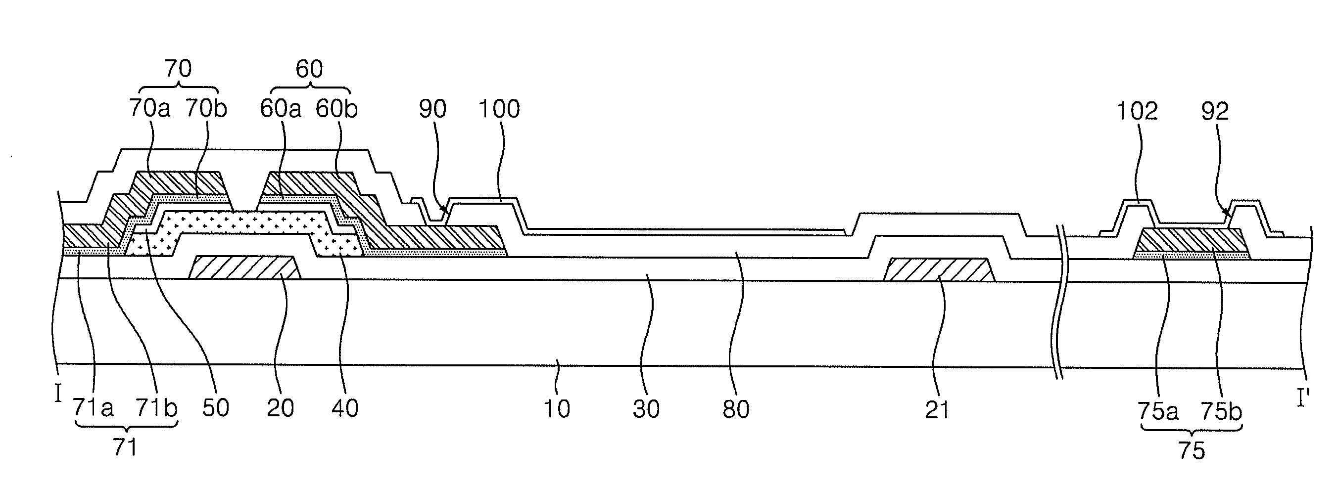
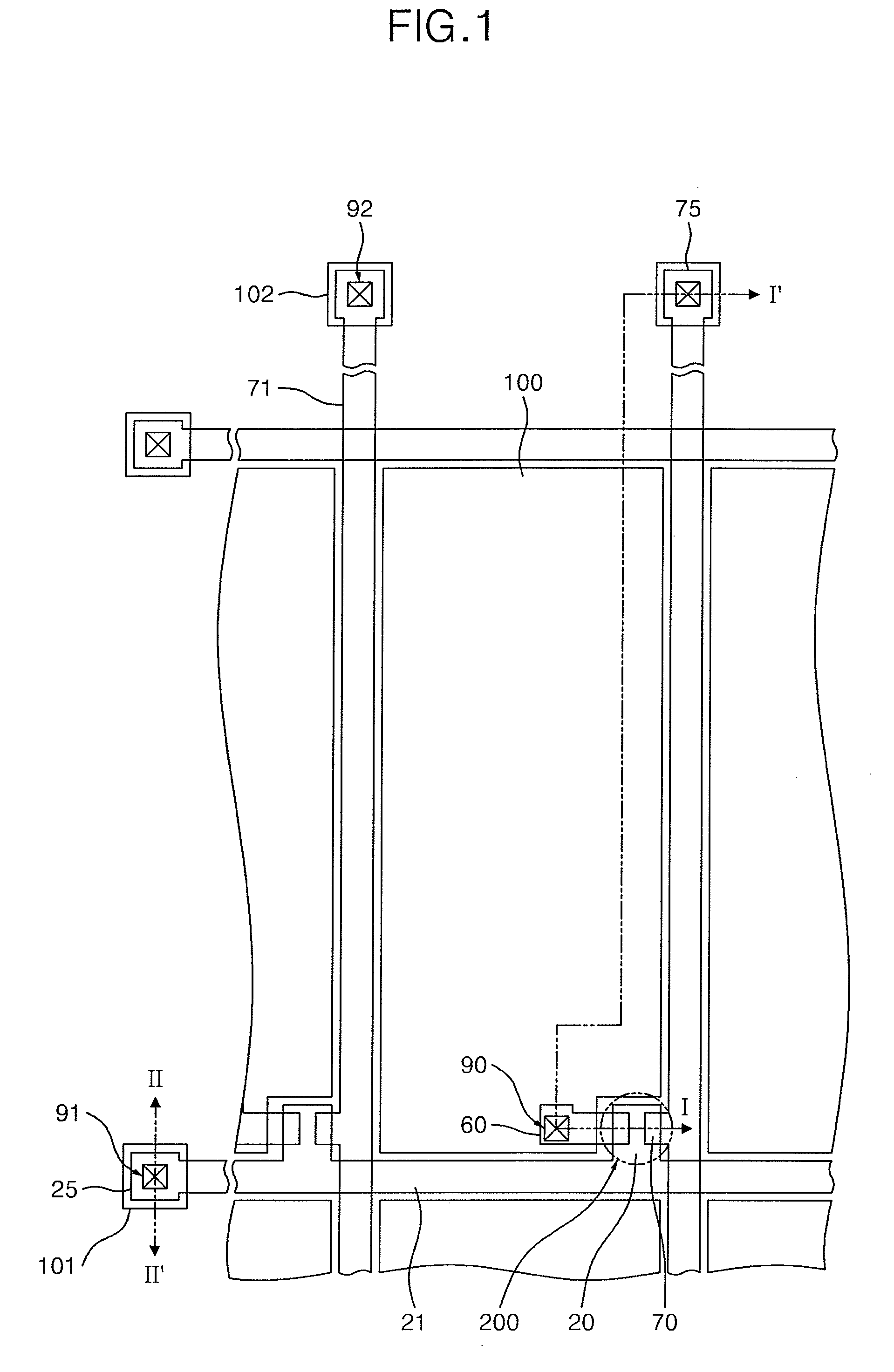
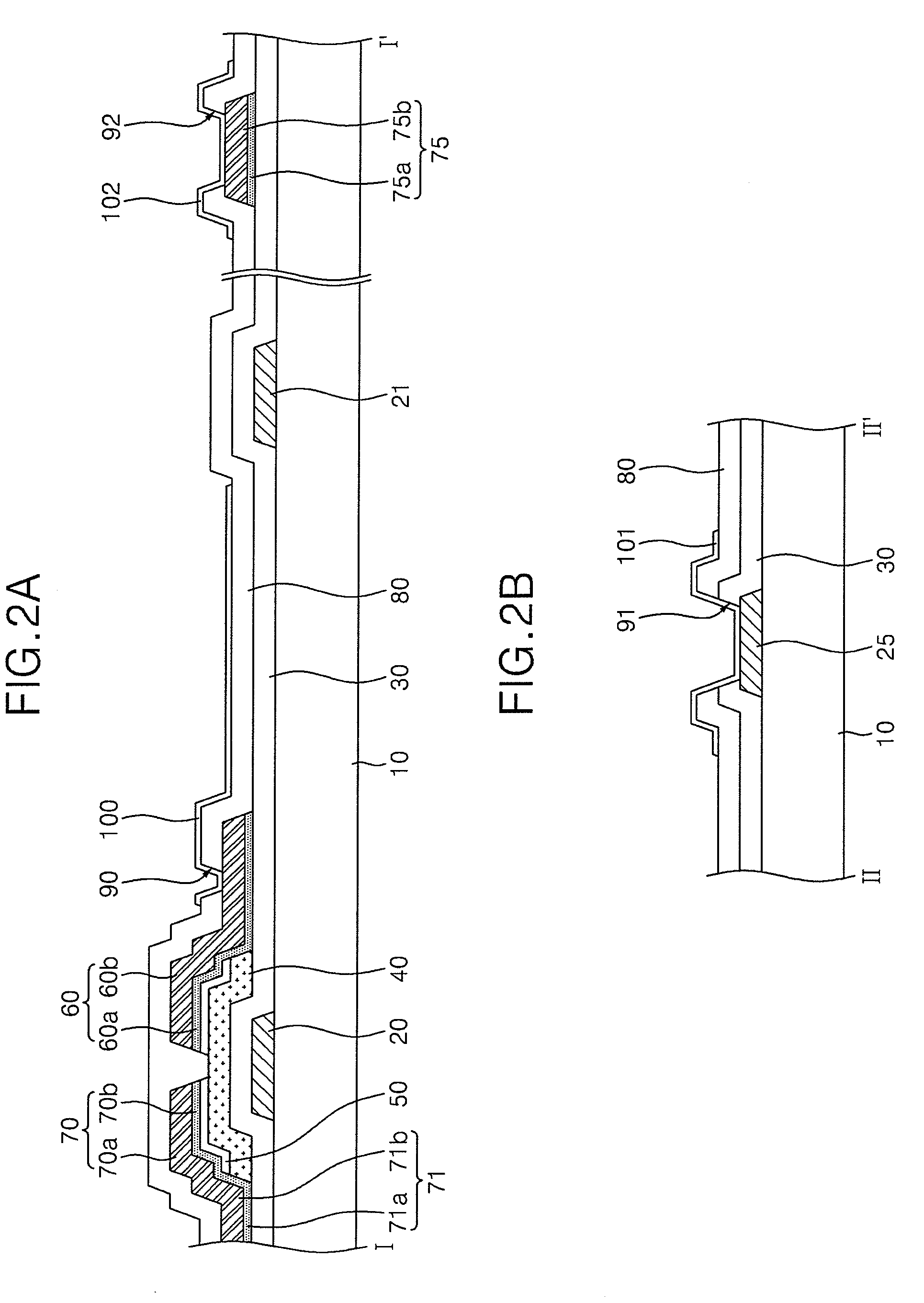
[0050]FIG. 1 is a plan view of a thin film transistor (“TFT”) substrate according to an exemplary embodiment of the present invention and FIGS. 2A and 2B are cross-sectional views taken along lines I-I′ and II-II′ of the TFT substrate in FIG. 1.

[0051]Referring to FIGS. 1, 2A and 2B, a TFT substrate includes gate lines 21 and data lines 71 intersecting each other and insulated by a gate insulating layer 30 to form pixel areas on a substrate 10. A pixel area includes a pixel electrode 100 and a TFT 200. A gate contact pad 25 is formed on an end of the gate line 21 and connected to a gate driving unit, and a first pad electrode 101 is coupled to the gate contact pad 25. A data contact pad 75 is formed on an end of the data line 71 and...


PUM

PropertyMeasurementUnit
etch rateaaaaaaaaaa
etch ratesaaaaaaaaaa

Abstract

A thin film transistor showing desirable contact characteristics during contact with indium tin oxide (ITO) or indium zinc oxide (IZO), in which a first conductive pattern including a gate electrode and a second conductive pattern including a source electrode and a drain electrode are formed without an etching process, a TFT substrate including the TFTs, and a method of manufacturing the same. The thin film transistor includes a gate electrode formed of a first conductive layer, a gate insulating layer covering the gate electrode, a semiconductor layer forming a channel on the gate insulating layer; an ohmic contact layer formed on the semiconductor layer, and a source electrode and a drain electrode formed of a second conductive layer and of a third conductive layer. The second conductive layer includes an aluminum-nickel alloy and nitrogen and is formed on the semiconductor layer. The third conductive layer includes an aluminum-nickel alloy and is formed on the second conductive layer.

Description

CROSS-REFERENCE TO RELATED APPLICATION[0001]This application is a Divisional Application of U.S. patent application Ser. No. 11 / 932,314 filed on Oct. 31, 2007, which claims priority to Korean Patent Application No. 10-2006-0116987, filed on Nov. 24, 2006, the disclosures of which are incorporated herein by reference in their entireties.BACKGROUND OF THE INVENTION[0002]1. Technical Field[0003]The present invention relates to a thin film transistor (“TFT”) substrate and a method of manufacturing the same and, more particularly, to a TFT that can directly contact indium tin oxide (“ITO”) or indium zinc oxide (“IZO”) and has desirable voltage-current characteristics, a TFT substrate including the TFTs, and a method of manufacturing the same.[0004]2. Discussion of the Related Art[0005]A TFT substrate is used as a circuit substrate for driving respective pixels in a flat panel display device such as a liquid crystal display (“LCD”) device, an organic light emitting diode (“OLED”) display ...

Claims


Application Information

Patent Timeline
Patent Type & Authority Applications(United States)
IPC IPC(8): H01L21/336
CPCH01L27/124H01L29/458H01L27/1214
Inventor BAE, YANG-HOJEONG, CHANG-OHKIM, BYEONG-BEOM
Owner SAMSUNG DISPLAY CO LTD
Why Eureka
Try Eureka