Nanoparticle based inorganic bonding material

a bonding material and nanoparticle technology, applied in semiconductor/solid-state device manufacturing, semiconductor devices, electrical equipment, etc., can solve the problems of limited photo-thermal stability, limited power of led-chips, and low light extraction efficiency between chips and optics of packages, and achieve high photo-thermal stability

Inactive Publication Date: 2010-02-04
KONINKLIJKE PHILIPS ELECTRONICS NV
View PDF5 Cites 7 Cited by
  • Summary
  • Abstract
  • Description
  • Claims
  • Application Information

AI Technical Summary

Benefits of technology

[0010]It is an object of the present invention to overcome this problem, and to provide a light-emitting device in which the LED-chip is bonded to the extraction optics by a bonding material that exhibits high photo-thermal stability, and which may be formed at temperatures not detrimental to the LED-chip

Problems solved by technology

The light extraction efficiency between the chips and the optics of the package is a major issue with which LEDs are confronted.
However, these optical domes have limited photo-thermal stability, which limits the power of the used LED-chips, which in turn limits the lumen power of the light-emitting device.
Another challenge is to have the optics such that they withstand high optical power at elevated temperatures, thus enabling high lumen power light sources by using high power LEDs, which dissipate a lot of heat when in operation.
However, high power LEDs may dissipate significant amounts of heat, and the radiation may be intense.
A complicating factor is that the LED-chips themselves only sustain moderate processing temperatures whilst materials with high photo-thermal stability are inorganic and typically are processed at too high temperature for the LED chips.

Method used


Image

  • Nanoparticle based inorganic bonding material
  • Nanoparticle based inorganic bonding material

Examples


Embodiment Construction

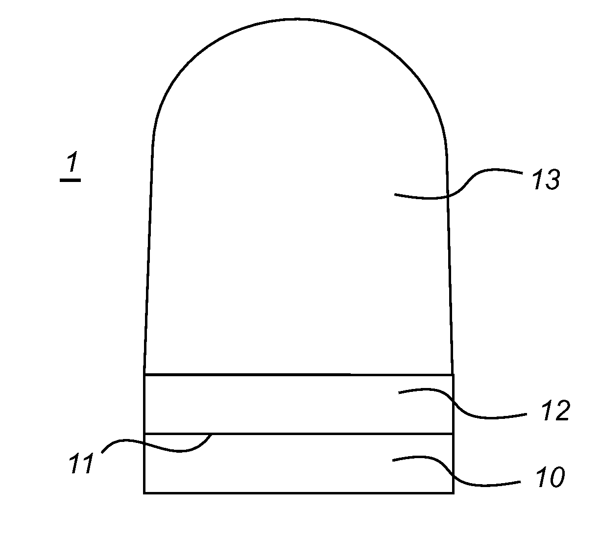
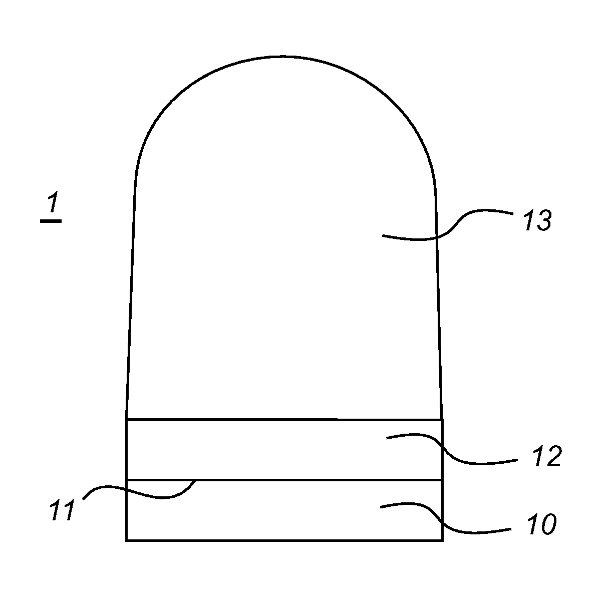
[0027]FIG. 1 shows a light-emitting device 1 according to an embodiment of the invention. The light-emitting device 1 may for example be used for illumination purposes. It comprises a light emitting diode (LED) chip 10, which is connected to an optical element 13 by means of a bond 12, such that the bond 12 couples the light emitted by the LED chip 10 from a light-emitting surface 11 of the LED chip to the optical element 13.

[0028]The optical element 13 in FIG. 1 is an optical dome for extracting light from the LED-chip. However, the optical element 13 may adopt other forms, for example it may be designed as a plate. The optical element may be of an organic material (for example PMMA), silicone, or of an inorganic material, such as a polycrystalline ceramic material or glass. Preferably, the optical element is of a material that is stable with regards to light of the wavelengths emitted by the underlying LED, and with regards to the temperatures achieved in the device during operati...


PUM

PropertyMeasurementUnit
mean particle sizeaaaaaaaaaa
temperatureaaaaaaaaaa
refractive indexaaaaaaaaaa

Abstract

A method for the production of a light emitting device is provided, comprising providing at least one LED 10 and at least one optical element 13; arranging a bonding material 12, comprising a stable colloidal sol of inorganic metal oxide nanoparticles dispersed in a liquid medium, on a light emitting surface 11 of said at least one LED and/or on a surface of said at least one optical element 13; (c) placing said at least one optical element 13 on the light emitting surface 11 of said at least one LED 10 with said bonding material 12 there between to form at least one assembly; and curing said bonding material to form an inorganic bond.
The bonding material may be cured at temperatures not detrimental to the LED, while the resulting bond is photo-thermally stable.

Description

FIELD OF THE INVENTION[0001]The present invention relates to a method for producing light emitting devices, as well as light emitting devices obtainable by such methods, and to the use of a stable colloidal sol of metal oxide nanoparticles as a bonding material precursor for bonding optical elements to light emitting diodes.BACKGROUND OF THE INVENTION[0002]Light emitting diodes (LEDs) are currently contemplated as light sources for several different lighting applications, and the use of light emitting diodes is expected to grow in the coming years.[0003]A light emitting diode is typically comprised in a package containing the actual LED-chip comprising the active, light producing, layers, and light extraction optics arranged on the LED-chip. The light extraction efficiency between the chips and the optics of the package is a major issue with which LEDs are confronted.[0004]A classical approach in this context involves the use of primary extraction optics, e.g. optical domes provided...

Claims


Application Information

Patent Timeline
Patent Type & Authority Applications(United States)
IPC IPC(8): H01L33/00H01L21/50H01L33/44H01L33/58
CPCH01L33/44H01L27/15H01L33/58
Inventor POPOVICI, MIHAELA-IOANAVERSCHUUREN, MARCUS ANTONIUSKLEYNEN, CHRISTIANGRAAF, JAN
Owner KONINKLIJKE PHILIPS ELECTRONICS NV
Why Eureka
Try Eureka