Solid-state image capturing device, method for manufacturing the same and electronic information device

a solid-state image and capture device technology, applied in the direction of radio frequency controlled devices, instruments, television systems, etc., can solve the problems of not only deteriorating the luminance shading characteristic, but also different luminance shading characteristics in each pixel, so as to improve the light receiving sensitivity and luminance shading characteristic, improve the uniformity and improve the effect of luminance shading characteristi

Inactive Publication Date: 2010-02-04
SHARP KK
View PDF4 Cites 15 Cited by
  • Summary
  • Abstract
  • Description
  • Claims
  • Application Information

AI Technical Summary

Benefits of technology

[0024]The present invention is intended to solve the conventional problems described above. The objective of the present invention is to provide: a solid-state image capturing device which is capable of preventing the reduction of the sensitivity with respect to the light of an image including oblique incident light, capable of preventing the decrease and the ununiformity of the luminance shading characteristic, also capable of making light of an image to be optimally incident in accordance of the location of a photodiode and which is easily processed; a method for manufacturing the solid-state image capturing device; and an electronic information device using the solid-state image capturing device for an image capturing section thereof.
[0055]According to the present invention, a plurality of microlenses are formed such that at least a part of the circumferential portions of the microlenses which are arranged above respective light receiving sections overlap or are in contact with adjacent microlenses. The locations of the microlenses in each pixel unit are different according to a sequence. In a solid-state image capturing device having the locations of adjacent light receiving sections in each pixel unit differ according to a sequence, the locations of microlenses in each pixel unit arranged above respective light receiving sections are different according to a sequence in a direction in which the locations of the light receiving sections in each pixel unit are arranged. As such, light that is incident upon each of the microlenses is incident upon approximately the same position (e.g., central portion or center) on the corresponding light receiving section. Therefore, it is possible to improve the light receiving sensitivity and the luminance shading characteristic, and also possible to improve the uniformity of the luminance shading characteristic.
[0056]By forming microlenses in a plurality of steps, it is possible to easily set the microlenses at the optimal positions, respectively, while maintaining the quality of microlenses, in consideration of the location, light receiving sensitivity and luminance shading characteristic of each of the photodiodes.
[0057]As described above, according to the present invention, in a solid-state image capturing device having the locations of adjacent light receiving sections in each pixel unit be different according to a sequence, the locations of the microlenses in each pixel unit are different according to a sequence in a direction in which the locations of the light receiving sections are in each pixel unit are different according to a sequence. As such, it is possible to improve the light receiving sensitivity in each pixel and also possible to improve the luminance shading characteristic in each pixel. In addition, light of an image can be incident upon approximately the same position on each of the light receiving sections. Therefore, it is possible to make the luminance shading characteristic uniform in the pixels having different locations according to a sequence in each pixel unit.

Problems solved by technology

As such, it is difficult to improve the luminance shading characteristic in every pixel at the same time.
As a result, problems of not only deteriorating the luminance shading characteristic, but also making the luminance shading characteristic different in each pixel occur.

Method used


Image

  • Solid-state image capturing device, method for manufacturing the same and electronic information device
  • Solid-state image capturing device, method for manufacturing the same and electronic information device
  • Solid-state image capturing device, method for manufacturing the same and electronic information device

Examples


embodiment 1

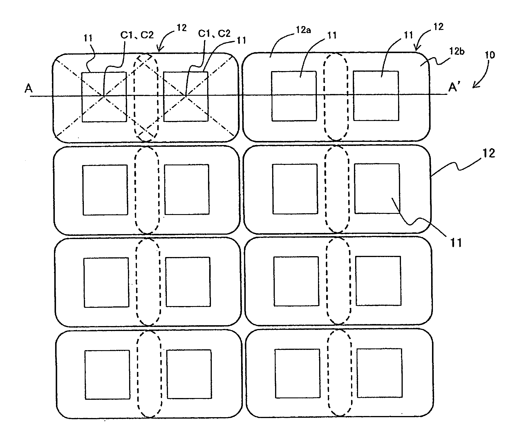
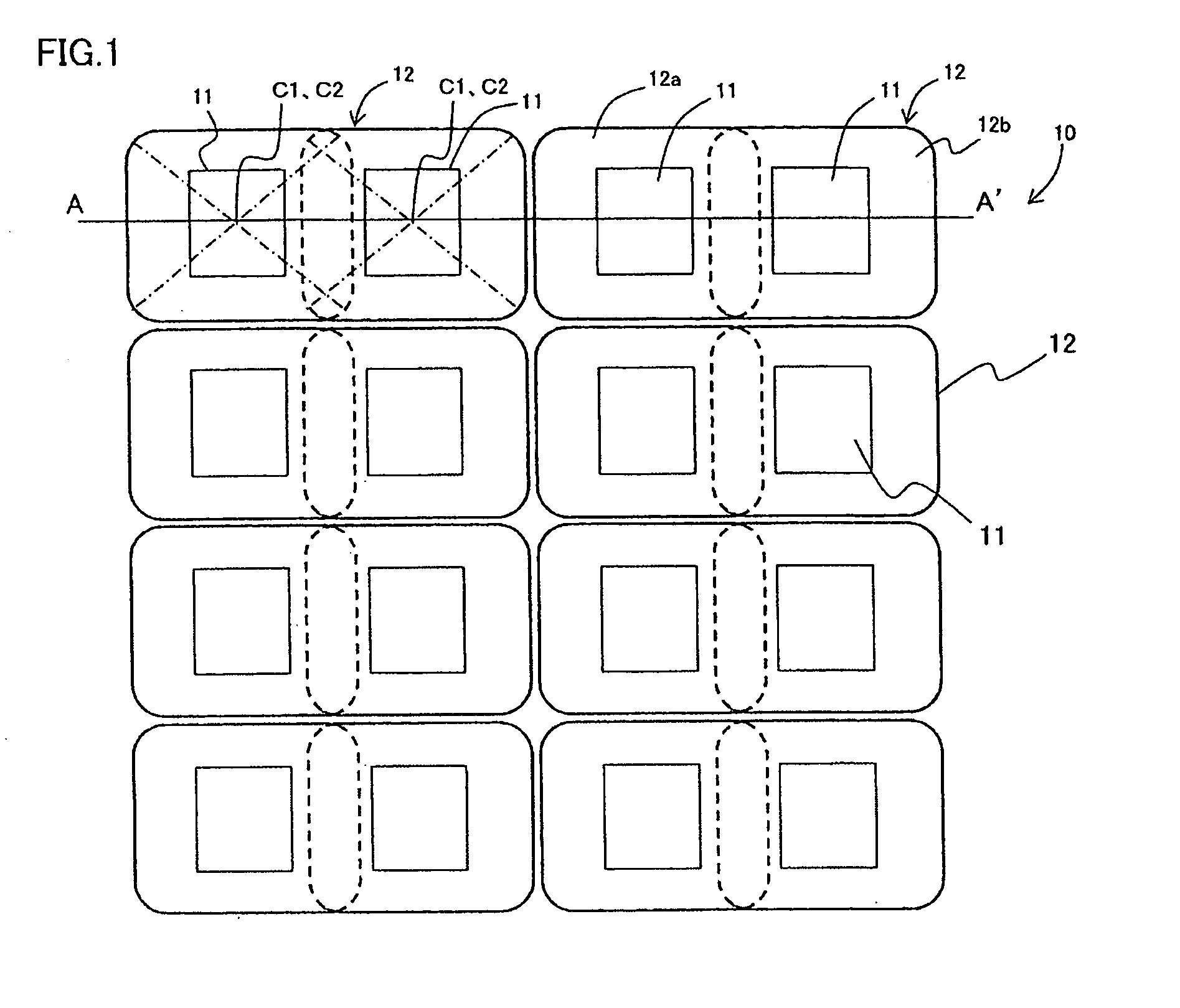
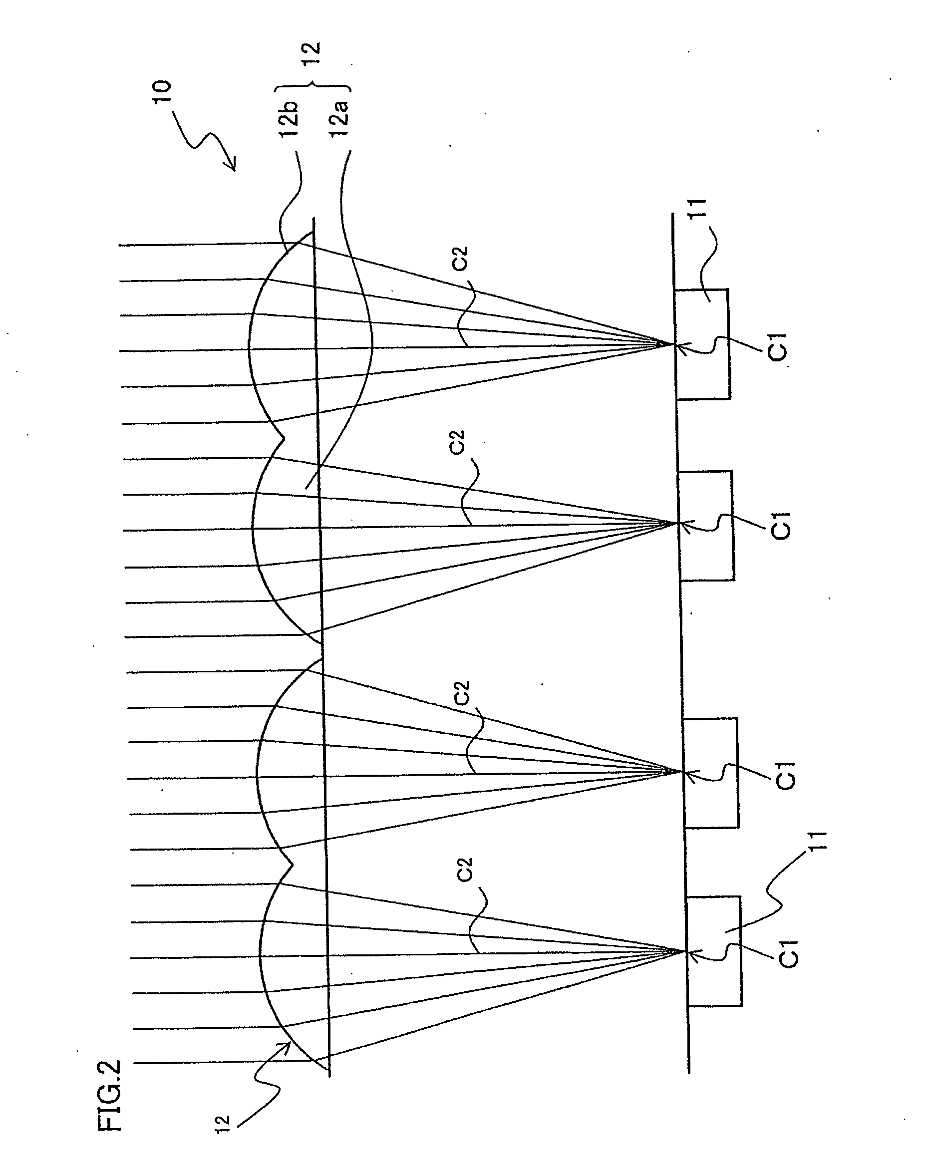
[0085]FIG. 1 is a plane view showing an exemplary essential structure of a pixel section in a solid-state image capturing device 10 according to Embodiment 1 of the present invention. FIG. 2 is a longitudinal cross-sectional view schematically showing a portion cut at line A-A′ in FIG. 1.

[0086]In FIG. 1 and FIG. 2, the solid-state image capturing device 10 according to Embodiment 1 includes: a plurality of photodiodes 11 as a plurality of light receiving sections arranged such that the locations thereof in each pixel unit are different according to a sequence; and microlens 12 arranged above the plurality of photodiodes 11 so as to correspond to the plurality of photodiodes 11. When some or all of the adjacent microlenses 12 among the microlenses 12 are close to each other such that the peripheral portions of the microlenses 12 overlap, the microlenses 12 having a shape of lens with the overlapped lens portions thereof straightly cut off are formed so the microlens 12 are adjacent t...

embodiment 2

[0100]Embodiment 2 will describe a case in which the first microlens 2a and the second microlens 2b according to Embodiment 1 are circular (or approximate circular or elliptical) in a plane view, and the curvature thereof is constant.

[0101]FIG. 5 is a plane view showing an exemplary essential structure of a pixel section in a solid-state image capturing device 20 according to Embodiment 2 of the present invention. FIG. 6 is a longitudinal cross-sectional view schematically showing a portion cut at line B-B′ in FIG. 5.

[0102]In the solid-state image capturing device 20 according to Embodiment 2 in FIG. 5 and FIG. 6, microlenses 22 are arranged above photodiodes 21 making up pixels so as to correspond to the photodiodes 21. The locations of the photodiodes 21 are different according to a sequence in each pixel unit. In a plane view, the center position C1 of a photodiode 21 matches the optical axis C2 of a corresponding microlens 22. The curvature of a microlens 22 in the solid-state i...

embodiment 3

[0116]Embodiments 1 and 2 have described the case in which photodiodes 11 or 21 are grouped in two pixels, and the locations of the photodiodes 11 or 21 in each two-pixel unit are different according to a sequence only in a row direction (horizontal direction). Embodiment 3 will describe a case in which photodiodes are grouped in four pixels, and the locations of the photodiodes in each four-pixel unit are different according to a sequence in both a row direction (horizontal direction) and a column direction (vertical direction).

[0117]FIG. 8 is a plane view showing an exemplary essential structure of a pixel section in a solid-state image capturing device 30 according to Embodiment 3 of the present invention.

[0118]In the solid-state image capturing device 30 according to Embodiment 3 in FIG. 8, one microlens 32 is provided above four photodiodes 31 making up four pixels in a lateral direction and a longitudinal direction so as to correspond to the four photodiodes 31. This one micro...


PUM


Abstract

In a solid-state image capturing device having the locations of photodiodes in each pixel unit to be different according to a sequence, the light receiving sensitivity and the luminance shading characteristic are improved. A circumferential portion of a microlens 12 which is arranged above a corresponding photodiode 11 is formed so as to overlap an adjacent microlens 12 thereto, and the locations of microlenses 12 in each pixel unit are different according to a sequence. Light of an image that is incident upon each of the microlenses 12 is incident upon approximately the same portion (e.g., central portion) of each of the respective photodiodes 11.

Description

TECHNICAL FIELD[0001]The present invention relates to: a solid-state image capturing device in which the locations of adjacent photoelectrical conversion sections in each pixel unit are different according to a sequence, and the light of an image from a subject is photoelectrically converted at each of the photoelectrical conversion sections and is then image-captured as a pixel; a method for manufacturing the solid-state image capturing device and; and an electronic information device (e.g., digital camera (digital video camera, digital still camera or the like), image input camera, scanner, facsimile, cell phone device equipped with camera and the like) using the solid-state image capturing device as an image input device for an image capturing section thereof.BACKGROUND ART[0002]Recently, in a conventional solid-state image capturing device such as a CCD image sensor or CMOS image sensor, the reduction of the size of a pixel cell have been extensively performed. In particular, in...

Claims


Application Information

Patent Timeline
Patent Type & Authority Applications(United States)
IPC IPC(8): H01L31/0232H01L27/14H01L27/146H01L27/148H04N5/335H04N5/361H04N5/369
CPCH01L27/14627H04N5/335H01L27/14685H04N25/00
Inventor KONISHI, TOMOHIRO
Owner SHARP KK
Why Eureka
Try Eureka