Integrated Circuit Interconnect Method and Apparatus

a technology of integrated circuits and interconnections, which is applied in the direction of electrical apparatus, semiconductor devices, and semiconductor/solid-state device details, etc., can solve the problems of high temperature associated with reflow of solder bumps, increased overall cost of flip chip technology, and wet processing of semiconductor wafers, etc., to reduce the cost of flip chip packaging, eliminate solder bumping, and increase the reliability of flip chip packaging

Inactive Publication Date: 2010-02-04
IBM CORP
View PDF11 Cites 21 Cited by
  • Summary
  • Abstract
  • Description
  • Claims
  • Application Information

AI Technical Summary

Benefits of technology

[0008]Illustrative embodiments of the present invention provide techniques for forming high volume solder features on a substrate and employing the high volume solder features in forming CS connections, wherein substantially all, or at least a majority, of the solder forming the connections comes from the high volume solder features formed on the substrate. The high volume solder features may be formed on the substrate using, for ex

Problems solved by technology

In “standard” IC packaging, the interconnection between the die and the carrier is made using bond wires, which exhibit disadvantages, particularly in high-frequency applications (e.g., about one gigahertz and above).
Using conventional solder bumping technology, when solder bumps are formed on the substrate, the semiconductor wafer is exposed to wet processing and high temperature associated with reflow of the solder bumps.
In some cases, the choice of under bump metallurgy (UBM), which generally refers to the pad metallurgy used to protect the IC while making a good mechanical and electrical connection to the solder bump and the substrate, may be limited by the solder bumping process

Method used


Image

  • Integrated Circuit Interconnect Method and Apparatus
  • Integrated Circuit Interconnect Method and Apparatus
  • Integrated Circuit Interconnect Method and Apparatus

Examples


Embodiment Construction

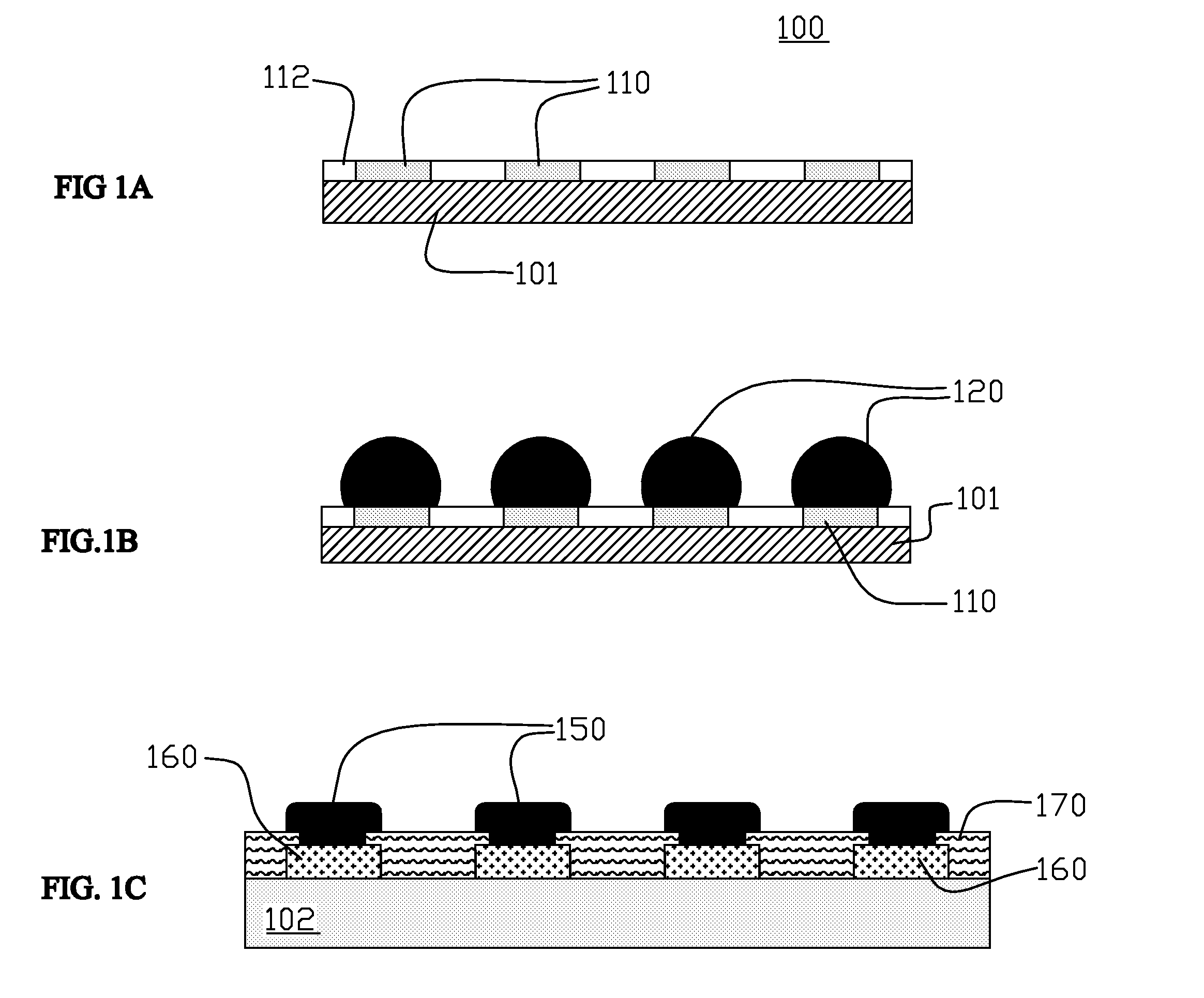
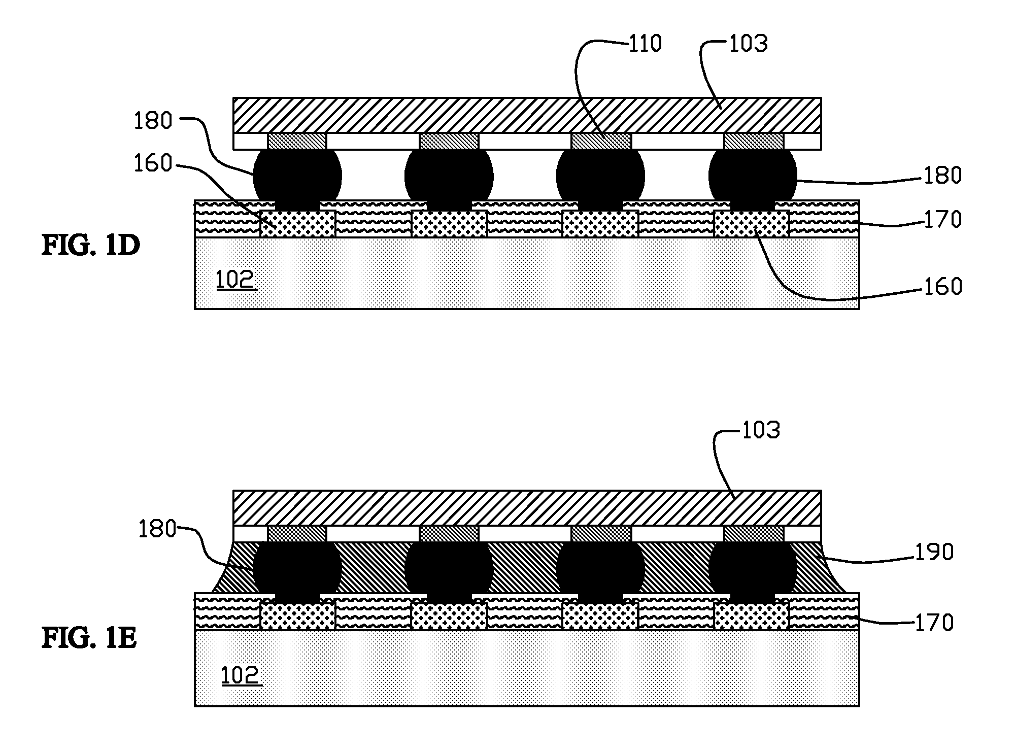
[0017]The present invention will be described herein in the context of illustrative embodiments of a methodology for forming high volume solder features on a substrate and an IC device employing same. It is to be appreciated, however, that the techniques of the present invention are not limited to the specific methods and device shown and described herein. Rather, embodiments of the invention are directed broadly to improved techniques for interconnecting an IC die to a substrate using high volume alloy deposits. For this reason, numerous modifications can be made to these embodiments and the results will still be within the scope of the invention. No limitations with respect to the specific embodiments described herein are intended or should be inferred.

[0018]Although combined in a novel manner, several of the processing steps described herein may be performed in conventional semiconductor processing, and, as result, will be familiar to those skilled in that art. Moreover, details ...


PUM


Abstract

Techniques for interconnecting an IC chip and a receiving substrate are provided. A method includes the steps of: providing the IC chip, the IC chip including at least a first connection site formed thereon; providing the receiving substrate, the receiving substrate including at least a second connection site formed thereon; forming an alloy structure on at least a portion of an upper surface of the second connection site; orienting the IC chip relative to the receiving substrate so that the at least first connection site is aligned with the alloy deposit formed on the at least second connection site; and forming an electrical connection between the first and second connection sites, the electrical connection comprising a volume of electrically conductive fusible material, wherein a majority of the volume of electrically conductive fusible material is supplied from the alloy structure.

Description

CROSS-REFERENCE TO RELATED APPLICATION(S) [0001]This application is a divisional of pending U.S. application Ser. No. 12 / 181,882, filed Jul. 29, 2008, the disclosure of which is incorporated by reference herein.FIELD OF THE INVENTION [0002]The present invention relates generally to electrical and electronic devices, and more particularly relates to semiconductor packaging and interconnection.BACKGROUND OF THE INVENTION [0003]Flip chip technology, first introduced in the 1960's by IBM as the controlled collapse chip connection (C4) process, offers a viable and proven alternative to standard assembly technologies for products requiring enhanced performance. Flip chip is not a specific package (like small-outline integrated circuit (SOIC)), or even a package type (like ball grid array (BGA)). Rather, flip chip generally describes the method of electrically connecting an integrated circuit (IC) die, also referred to as a chip, to a package carrier. The package carrier, either substrate ...

Claims


Application Information

Patent Timeline
IPC IPC(8): H01L23/50
CPCH01L21/563H01L21/6835H01L2924/10253H01L2924/01087H01L2924/01075H01L2924/01055H01L23/49811H01L23/49816H01L23/49894H01L24/11H01L24/12H01L24/16H01L24/81H01L2224/11003H01L2224/16225H01L2224/81101H01L2224/81192H01L2224/8121H01L2224/81815H01L2924/01082H01L2924/01322H01L2924/14H01L2224/13111H01L2924/01006H01L2924/01033H01L2924/0105H01L2924/00H01L2224/11334
Inventor GRUBER, PETER ALFREDNAH, JAE-WOONG
Owner IBM CORP
Why Eureka
Try Eureka