Wafer Level Interconnection of Inverted Metamorphic Multijunction Solar Cells

a solar cell and inverted metamorphic technology, applied in the field of solar cell semiconductor devices and multifunctional solar cells, can solve the problems of assembly costs, yield losses, and possible less than ideal packing density, and achieve the effect of improving the efficiency of solar cells and reducing the cost of assembly

Active Publication Date: 2010-02-11
SOLAERO TECH CORP
View PDF94 Cites 66 Cited by
  • Summary
  • Abstract
  • Description
  • Claims
  • Application Information

AI Technical Summary

Benefits of technology

[0026]In another aspect, the present invention provides a multijunction solar cell array comprising a plurality of solar cells mounted on a carrier, each solar cell including (i) a first solar subcell having a first band gap, (ii) a second solar subcell disposed over the first solar subcell having a second band gap smaller than the first band gap, (iii) a graded interlayer disposed over the second ...

Problems solved by technology

While significant progress has been made in this area, the requirement for solar cells to meet the needs of more sophisticated applications has not kept pace with demand.
The structures described in such reference present a number of practical di...

Method used


Image

  • Wafer Level Interconnection of Inverted Metamorphic Multijunction Solar Cells
  • Wafer Level Interconnection of Inverted Metamorphic Multijunction Solar Cells
  • Wafer Level Interconnection of Inverted Metamorphic Multijunction Solar Cells

Examples


second embodiment

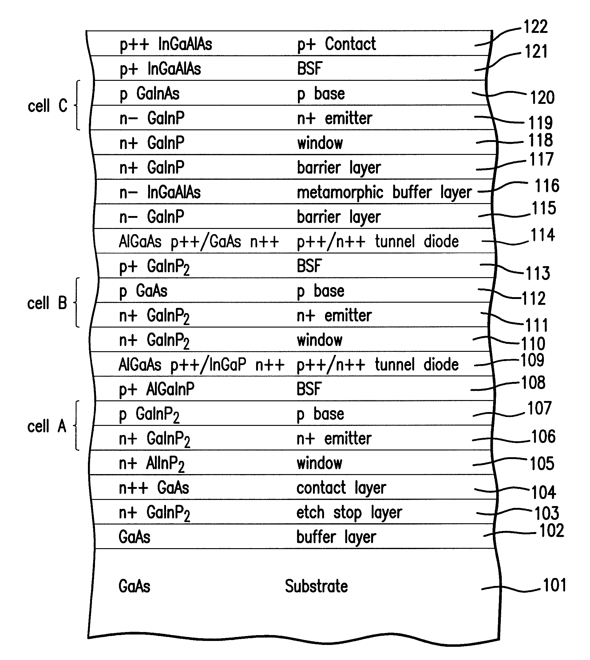
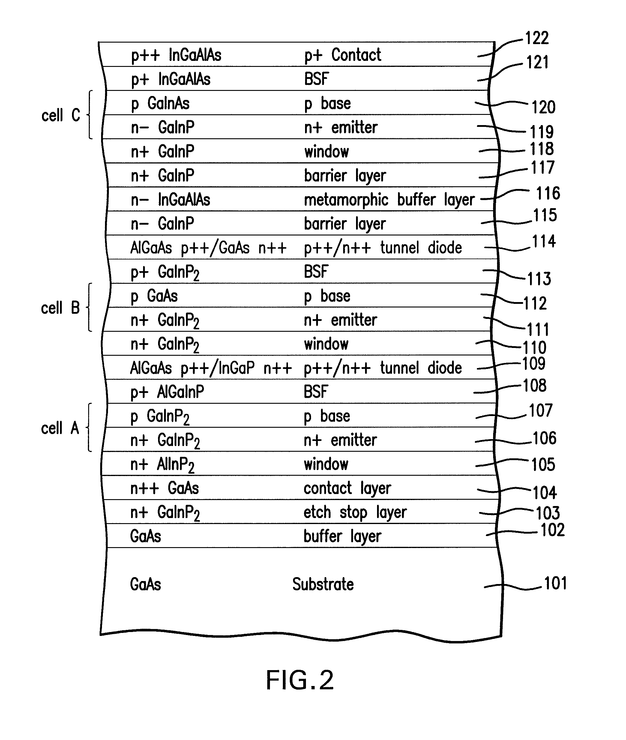
[0079]Although the preferred embodiment of the present invention utilizes a plurality of layers of InGaAlAs for the metamorphic layer 116 for reasons of manufacturability and radiation transparency, other embodiments of the present invention may utilize different material systems to achieve a change in lattice constant from subcell B to subcell C. Thus, the system of Wanlass using compositionally graded InGaP is the present invention. Other embodiments of the present invention may utilize continuously graded, as opposed to step graded, materials. More generally, the graded interlayer may be composed of any of the As, P, N, Sb based III-V compound semiconductors subject to the constraints of having the in-plane lattice parameter greater or equal to that of the second solar cell and less than or equal to that of the third solar cell, and having a bandgap energy greater than that of the second solar cell.

[0080]In another embodiment of the present invention, an optional second barrier l...

first embodiment

[0102]FIG. 10C is a top plan view of a wafer in which the solar cells are interconnected according to the present invention in which wire bonds are used as the electrical interconnects. More specifically, wire bond 708 electrically connects the bottom contact pad 702 of cell 3 with the front contact pad 707 of cell 4. Similarly wire bond 709 connects bottom contact pad 705 of cell 4 and front contact pad 720 of cell 2, and wire bond 710 connects bottom contact pad 721 with front contact pad 503 of cell 1. The cross-sectional view of this wafer through the B-B plane is shown in FIG. 18.

[0103]FIG. 10D is a top plan view of a wafer in which the solar cells are interconnected according to a second embodiment of the present invention by a thin film metal interconnects.

[0104]More specifically,the Figure depicts the embodiment in which thin film interconnect 722 connects the bottom contact pad 702 of cell 3 with front contact pad 707 of cell 4. Similarly, thin film interconnect 723 connect...

third embodiment

[0112]FIG. 15 is a cross-sectional view of the solar cell of FIG. 14C after the next process step in the present invention in which a cover glass is secured to the top of the cell and the surrogate substrate 125 is entirely removed, leaving only the metal contact layer 123 which forms the backside contact of the solar cell. The surrogate substrate may be reused in subsequent wafer processing operations.

[0113]FIG. 16 is a graph of a doping profile in the emitter and base layers in one or more subcells of the inverted metamorphic multifunction solar cell of the present invention. The various doping profiles within the scope of the present invention, and the advantages of such doping profiles are more particularly described in copending U.S. patent application Ser. No. 11 / 956,069 filed Dec. 13, 2007, herein incorporated by reference. The doping profiles depicted herein are merely illustrative, and other more complex profiles may be utilized as would be apparent to those skilled in th...


PUM


Abstract

A method of forming a plurality of discrete, interconnected solar cells mounted on a carrier by providing a first semiconductor substrate; depositing on the first substrate a sequence of layers of semiconductor material forming a solar cell structure; forming a metal back contact layer over the solar cell structure; mounting a carrier on top of the metal back contact; removing the first substrate; and lithographically patterning and etching the solar cell structure to form a plurality of discrete solar cells mounted on the carrier.

Description

REFERENCE TO RELATED APPLICATIONS[0001]This application is related to co-pending U.S. patent application Ser. No. 12 / 218,582 filed Jul. 18, 2008.[0002]This application is related to co-pending U.S. patent application Ser. No. 12 / 218,558 filed Jul. 17, 2008.[0003]This application is related to co-pending U.S. patent application Ser. No. 12 / 123,864 filed May 20, 2008.[0004]This application is related to co-pending U.S. patent application Ser. No. 12 / 102,550 filed Apr. 14, 2008.[0005]This application is related to co-pending U.S. patent application Ser. No. 12 / 047,842, and U.S. Ser. No. 12 / 047,944, filed Mar. 13, 2008.[0006]This application is related to co-pending U.S. patent application Ser. No. 12 / 023,772, filed Jan. 31, 2008.[0007]This application is related to co-pending U.S. patent application Ser. No. 11 / 956,069, filed Dec. 13, 2007.[0008]This application is also related to co-pending U.S. patent application Ser. Nos. 11 / 860,142 and 11 / 860,183 filed Sep. 24, 2007.[0009]This appl...

Claims


Application Information

Patent Timeline
IPC IPC(8): H01L31/042H01L31/18
CPCH01L31/022425H01L31/06875H01L31/078H01L31/1892H01L31/0508Y02E10/544H01L31/046H01L27/1421H01L31/0504Y02E10/52H01L31/048H01L31/0687H01L31/0475
Inventor VARGHESE, TANSEN
Owner SOLAERO TECH CORP
Why Eureka
Try Eureka