

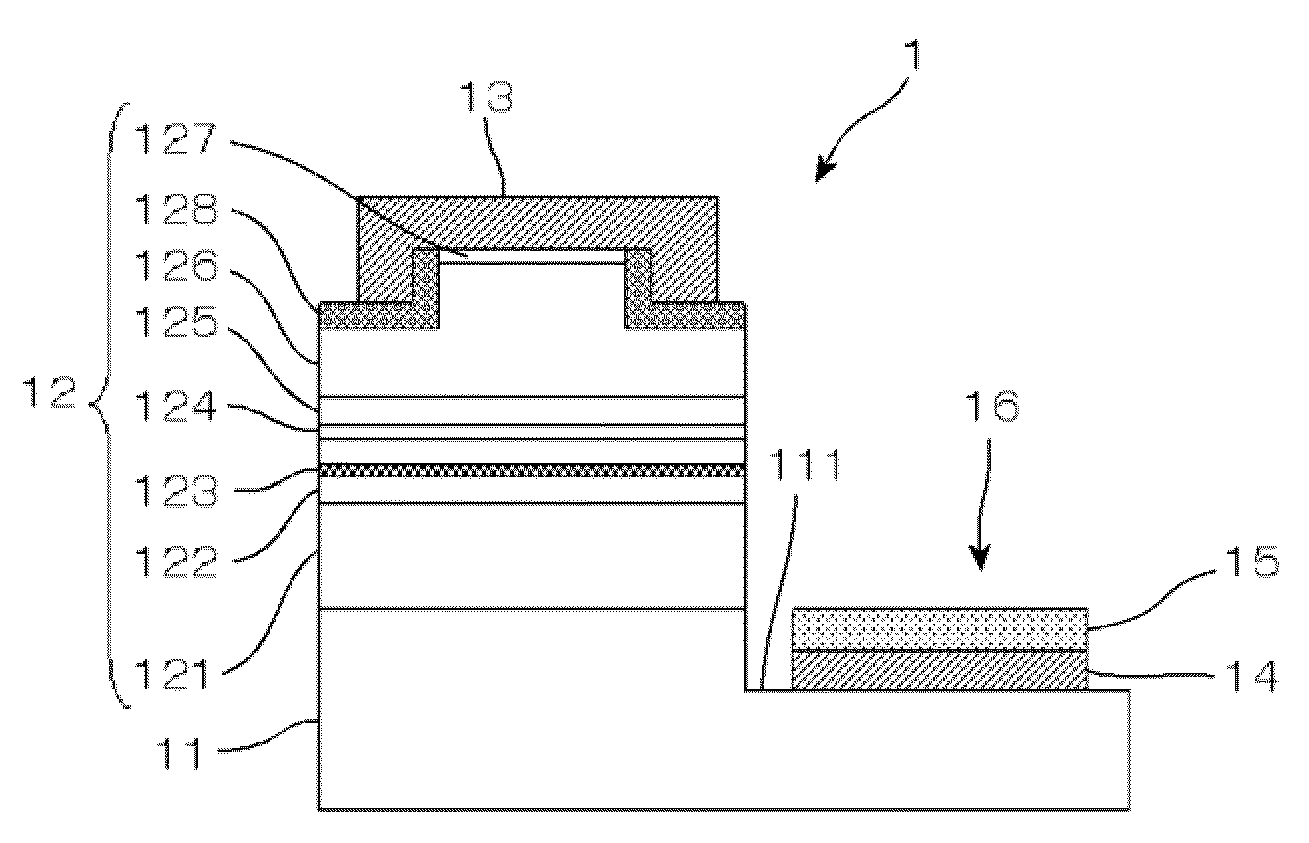
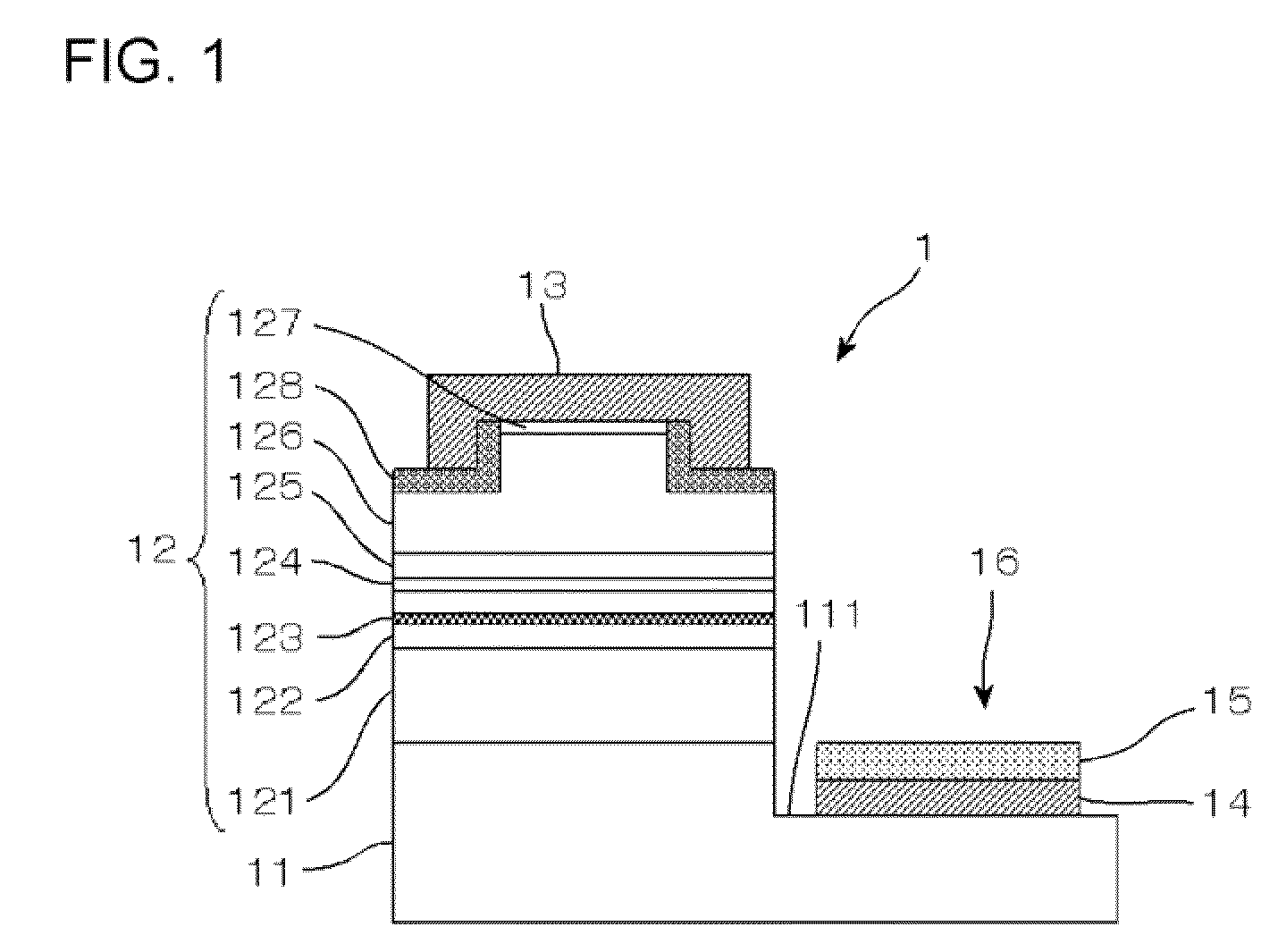
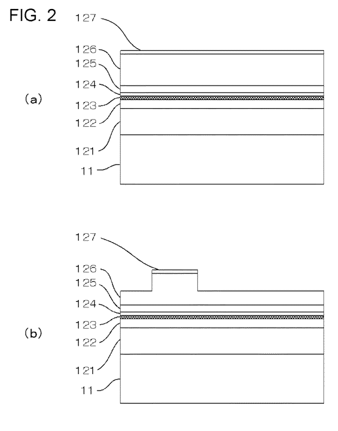
Electrode structure, semiconductor element, and methods of manufacturing the same
a semiconductor element and electrode structure technology, applied in the field of electrode structure, can solve the problems of n vacancies, ti atoms cannot efficiently combine with n atoms, and it is difficult to realize the electrode structure capable of satisfying the needs, so as to reduce the contact resistance between the electrode and the nitride semiconductor layer. the effect of reducing the contact resistan
- Summary
- Abstract
- Description
- Claims
- Application Information
AI Technical Summary
Benefits of technology
Problems solved by technology
Method used
Image

Examples
example 1
[0164]A semiconductor laser similar to that described in the first exemplary embodiment was manufactured, and relation between the temperature of annealing of the electrode structure and voltage was examined.
[0165]More specifically, the multi-layer film similar to that described in the first exemplary embodiment was formed over the GaN substrate, and the n-side electrode was formed. The first layer of the n-side electrode was configured by a layer composed of Ti, the second layer was configured by a layer composed of Nb, and the third layer was configured by a layer composed of Au, wherein the thickness of the second layer was set to 50 nm, and the thickness of the third layer was set to 100 nm. The thickness of the first layer was varied over the range from 5 to 100 nm, so as to form 6 types of n-side electrodes.
[0166]The GaN substrate having the n-side electrode formed thereon was annealed at different temperatures, to form the p-side electrode.
[0167]Voltage between the n-side ele...
PUM
 Abstract
Description
Claims
Application Information