Method for Manufacturing InGaN

a manufacturing method and ingan technology, applied in the direction of crystal growth process, monocrystalline material growth, semiconductor lasers, etc., to achieve the effect of improving the crystallinity of the ingan layer, reducing segregation, and increasing the proportion of in in the ingan layer

Inactive Publication Date: 2010-02-11
ROHM CO LTD
View PDF1 Cites 6 Cited by
  • Summary
  • Abstract
  • Description
  • Claims
  • Application Information

AI Technical Summary

Benefits of technology

[0011]According to the present invention, crystalline growth of the InGaN layer is performed at a flow rate of trimethylindium of 0.882×10⁻⁵ to 3.53×10⁻⁵ mol / min. This can reduce segregation of In and increase the proportion of In in the InGaN layer. Accordingly, the growth temperature of the InGaN layer can be increased, so that the crystallinity of the InGaN layer can be improved.

Problems solved by technology

However, when the InGaN layer is grown by the reaction rate controlling mode, TMIn is excessively flown, so that excess In which cannot be involved in the growth of the InGaN layer is segregated in the surface of the InGaN layer.

Method used


Image

  • Method for Manufacturing InGaN
  • Method for Manufacturing InGaN
  • Method for Manufacturing InGaN

Examples


Embodiment Construction

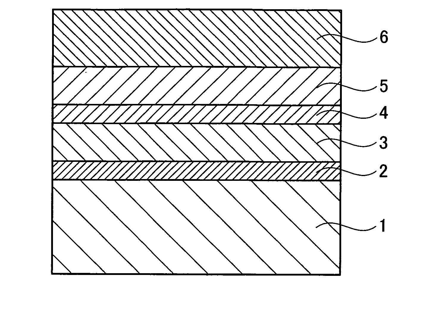
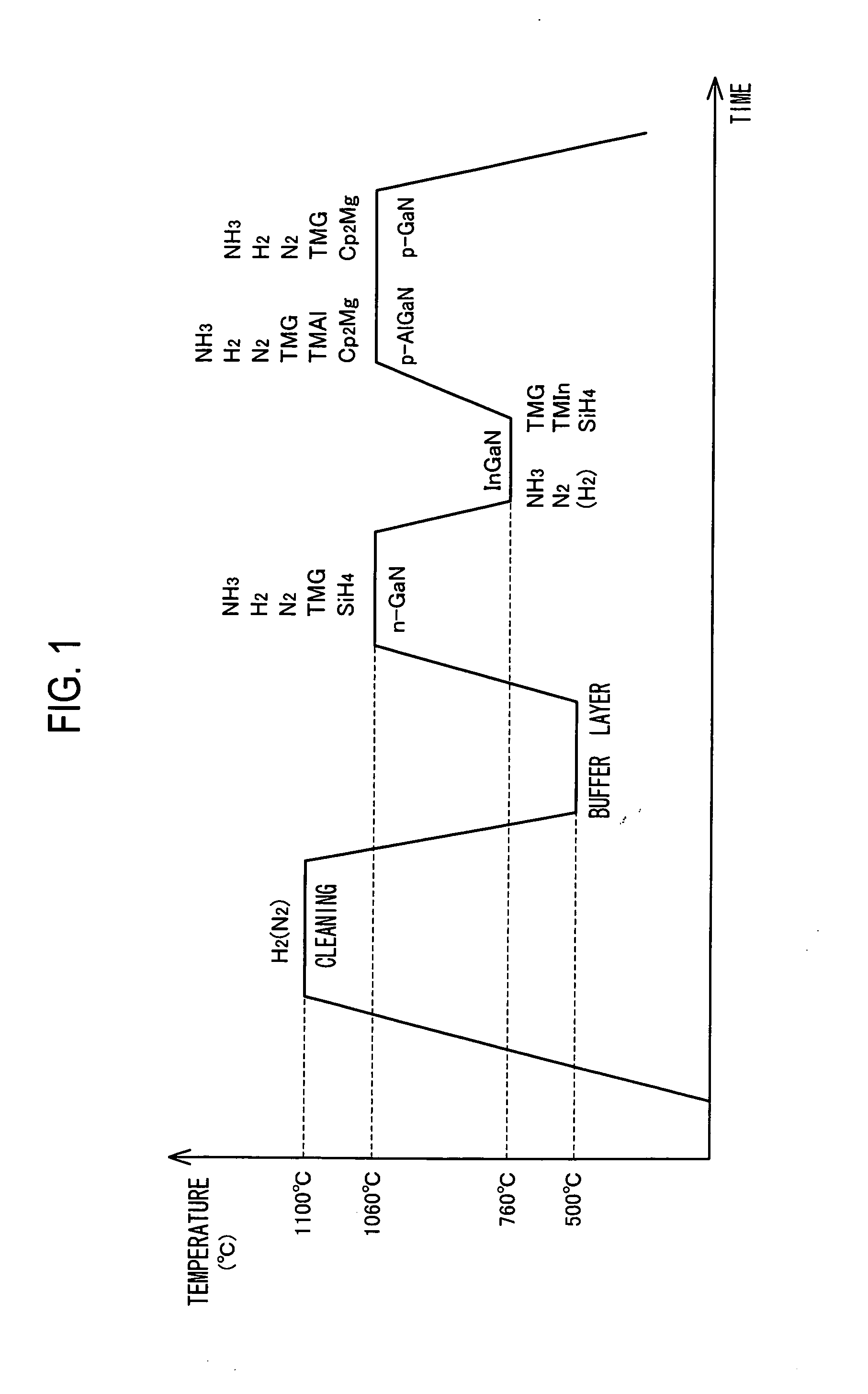
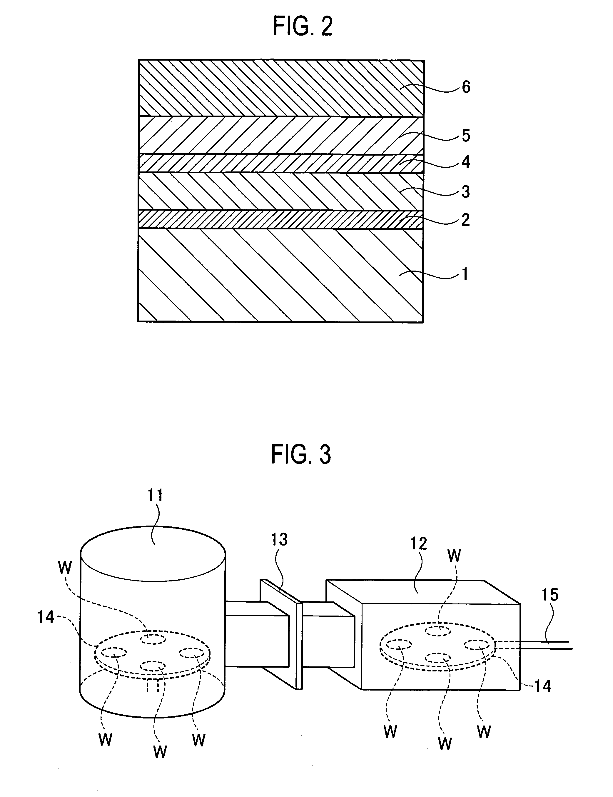
[0030]Hereinafter, a description is given of an embodiment of the present invention with reference to the drawings. FIG. 2 is a view showing a cross-sectional structure of a semiconductor light emitting device including an InGaN layer according to the present invention.

[0031]As shown in FIG. 2, the semiconductor light emitting device including the InGaN layer manufactured by a manufacturing method of the present invention includes a sapphire substrate 1, an n-type buffer layer 2, an n-GaN layer 3, an InGaN active layer 4, a p-AlGaN layer 5, and a p-GaN layer 6, which are stacked on each other.

[0032]FIG. 3 is a schematic view of a manufacturing apparatus for manufacturing the above semiconductor light emitting device. The manufacturing apparatus includes a growth chamber 11, a load lock chamber 12, and a valve 13 dividing the growth chamber 11 and load lock chamber 12.

[0033]The growth chamber 11 is always evacuated and is not set to atmospheric pressure. The load lock chamber 12 is s...


PUM

PropertyMeasurementUnit
Temperatureaaaaaaaaaa
Catalytic activityaaaaaaaaaa
Crystallinityaaaaaaaaaa

Abstract

To provide a method for manufacturing InGaN which causes less segregation of In and achieves high crystallinity of an InGaN layer with the proportion of In increased.The method for manufacturing an InGaN layer including growing an InGaN layer under conditions of a growth temperature of 700 to 790° C., a growth rate of 30 to 93 Å / min, and a flow rate of trimethylindium of 0.882×10⁻⁵ to 3.53×10⁻⁵ mol / min.

Description

TECHNICAL FIELD[0001]The present invention relates to a method for manufacturing InGaN for making semiconductor laser or the like.BACKGROUND ART[0002]As light source of optical information recording systems such as next-generation DVDs, semiconductor light emitting devices each including an active layer having an InGaN layer which can emit light in a violet-blue range and to which information can be written with high density have attracted attention.[0003]Generally, to manufacture a semiconductor light emitting device including an InGaN layer, an n-GaN layer is formed on a substrate, and the InGaN layer is then formed on the n-GaN layer. There are known various methods for manufacturing the InGaN layer. For example, one of the known manufacturing methods is a method by a reaction rate controlling mode in which the InGaN layer is formed with trimethylindium (hereinafter, referred to as TMIn) being excessively flown for purposes of increasing an amount of In incorporated in the InGaN ...

Claims


Application Information

Patent Timeline
IPC IPC(8): H01L21/20C23C16/34C30B29/38H01L21/205H01L33/32H01S5/323
CPCC23C16/303C30B25/02C30B29/403H01L21/0262H01L21/0254H01L21/02576H01L21/02579H01L21/0242
Inventor SONOBE, MASAYUKIITO, NORIKAZUTSUTSUMI, KAZUAKIFUJIWARA, TETSUYATAMAI, SHINICHI
Owner ROHM CO LTD
Why Eureka
Try Eureka