Thin-film transistor fabrication process and display device
- Summary
- Abstract
- Description
- Claims
- Application Information
AI Technical Summary
Benefits of technology
Problems solved by technology
Method used
Image

Examples
first embodiment
Reverse Stagger Type TFT
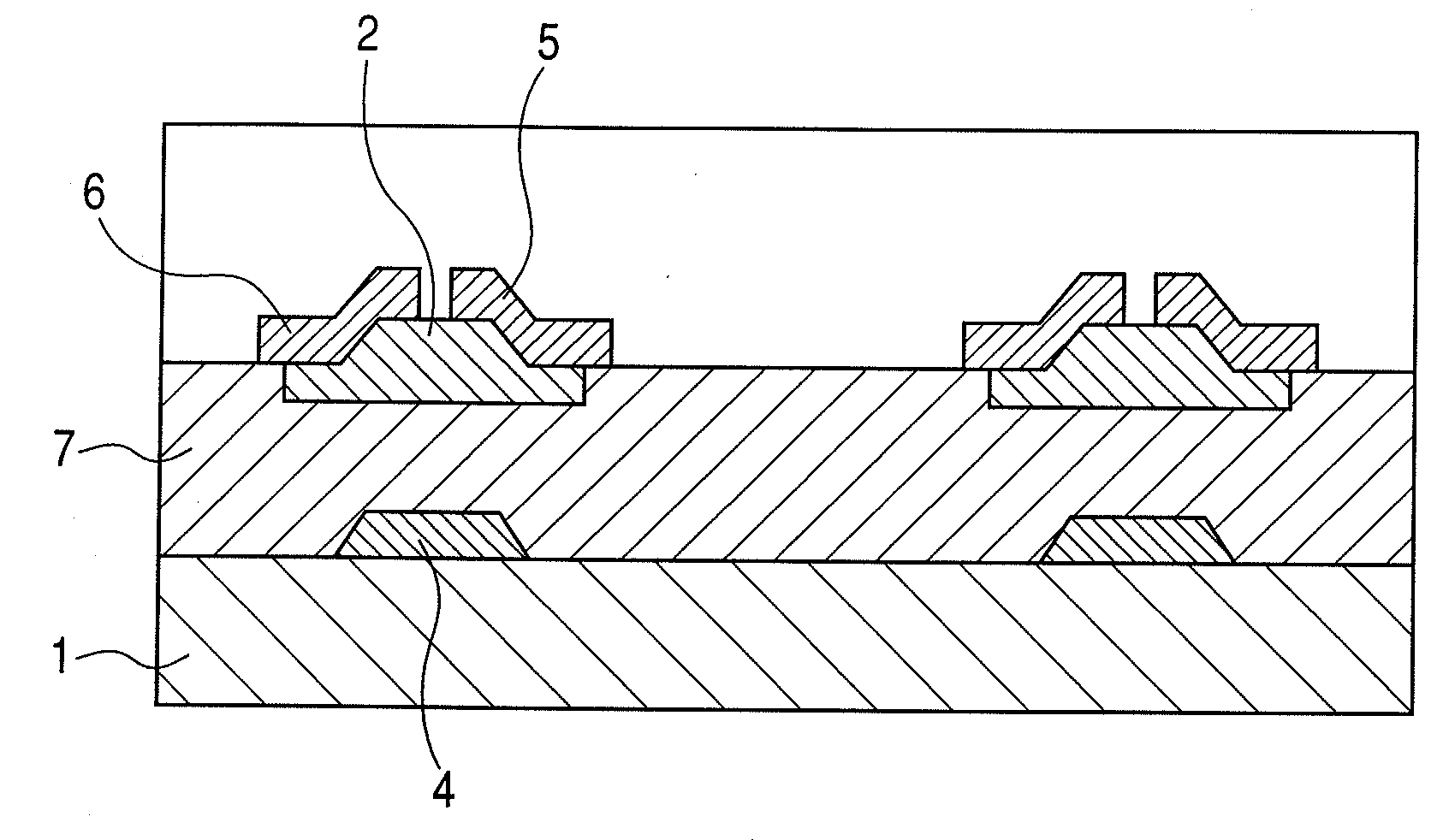
[0076]FIG. 1 is a sectional view showing the configuration of a thin-film transistor of bottom gate structure, as a thin-film transistor according to a first embodiment of the present invention.
[0077]A gate electrode 4 is provided on a substrate 1, and a high-resistance oxide layer 7 is provided thereon as the metal oxide layer, which shows a high resistivity of 1010 Ω·cm or more. On this layer 7, a source electrode 6 and a drain electrode 5 are provided. As materials for these electrodes, usable are, e.g., a metal selected from Mo, Ti, W and Al, or an alloy of any of these metals. For each electrode, at least one layer composed of any of these materials may be formed. Stated specifically, each electrode may be formed in three-layer structure in which a conductor composed of a metal having a relatively low resistance is held between top and bottom different conductors (such as Mo / W / Mo, Mo / Al / Mo, Ti / Al / Ti, Ti / Mo / Ti and MoW / Al / MoW).
[0078]Thereafter, on the basi...
second embodiment
Reverse Stagger Type TFT
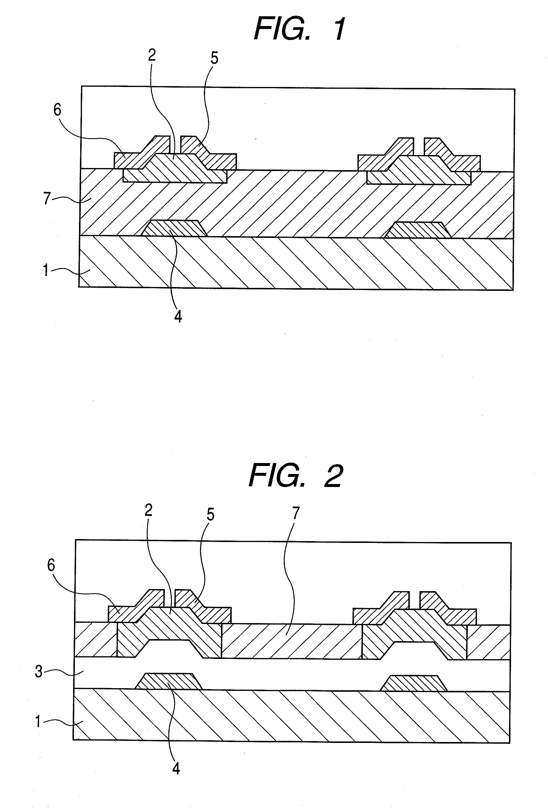
[0084]FIG. 2 is a sectional view showing the configuration of a thin-film transistor of bottom gate structure, as a thin-film transistor according to a second embodiment of the present invention.
[0085]A gate electrode 4 is provided on a substrate 1, and a gate insulating film 3 is further provided thereon. On this film 3, a high-resistance oxide layer 7 is provided as the metal oxide layer, which shows a high resistivity of 1010 Ω·cm or more. On this layer 7, a source electrode 6 and a drain electrode 5 are provided.
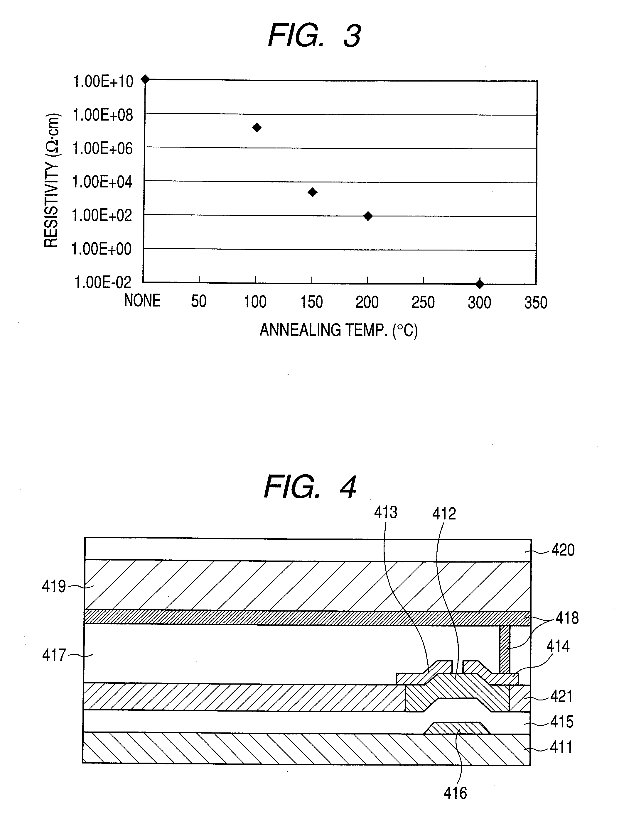
[0086]Thereafter, on the basis of changes in resistivity as shown in FIG. 3 which are caused when the high-resistance oxide layer is subjected to annealing in an inert gas, the annealing is carried out at a desired temperature to make part of the high-resistance oxide layer low in resistance to provide a channel region 2. He gas is used as the inert gas used when the annealing is carried out.
[0087]In this annealing, it is desirable to make the oxi...
third embodiment
[0091]To the drain electrode which is an output terminal of the above thin-film transistor, an electrode of a display element such as an electroluminescent (EL) element or a liquid-crystal element may be connected to make up a display device. Examples of how the display device is specifically made up are described below with reference to the drawings of display devices.
[0092]FIG. 4 is a sectional view showing an example of display device in which an electroluminescent element as a display element is used.
[0093]For example, as shown in FIG. 4, a gate electrode 416 and a gate insulating film 415 are formed on a substrate 411, and thereafter on the gate insulating film 415 a high-resistance oxide layer 421 is formed, which shows a high resistivity. Further, a source electrode 413 and a drain electrode 414 are formed, and thereafter the annealing is carried out in an inert gas to make part of the high-resistance oxide layer 421 low in resistance to provide a channel region...
PUM
 Abstract
Description
Claims
Application Information