PROCESS FOR PRODUCING LOCALISED Ge0I STRUCTURES, OBTAINED BY GERMANIUM CONDENSATION

a technology of localised geoi and germanium, which is applied in the direction of basic electric elements, electrical equipment, semiconductor devices, etc., can solve the problem of becoming a pollutan

Active Publication Date: 2010-02-25
COMMISSARIAT A LENERGIE ATOMIQUE ET AUX ENERGIES ALTERNATIVES
View PDF5 Cites 9 Cited by
  • Summary
  • Abstract
  • Description
  • Claims
  • Application Information

AI Technical Summary

Benefits of technology

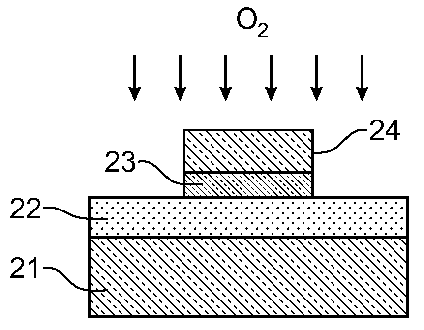
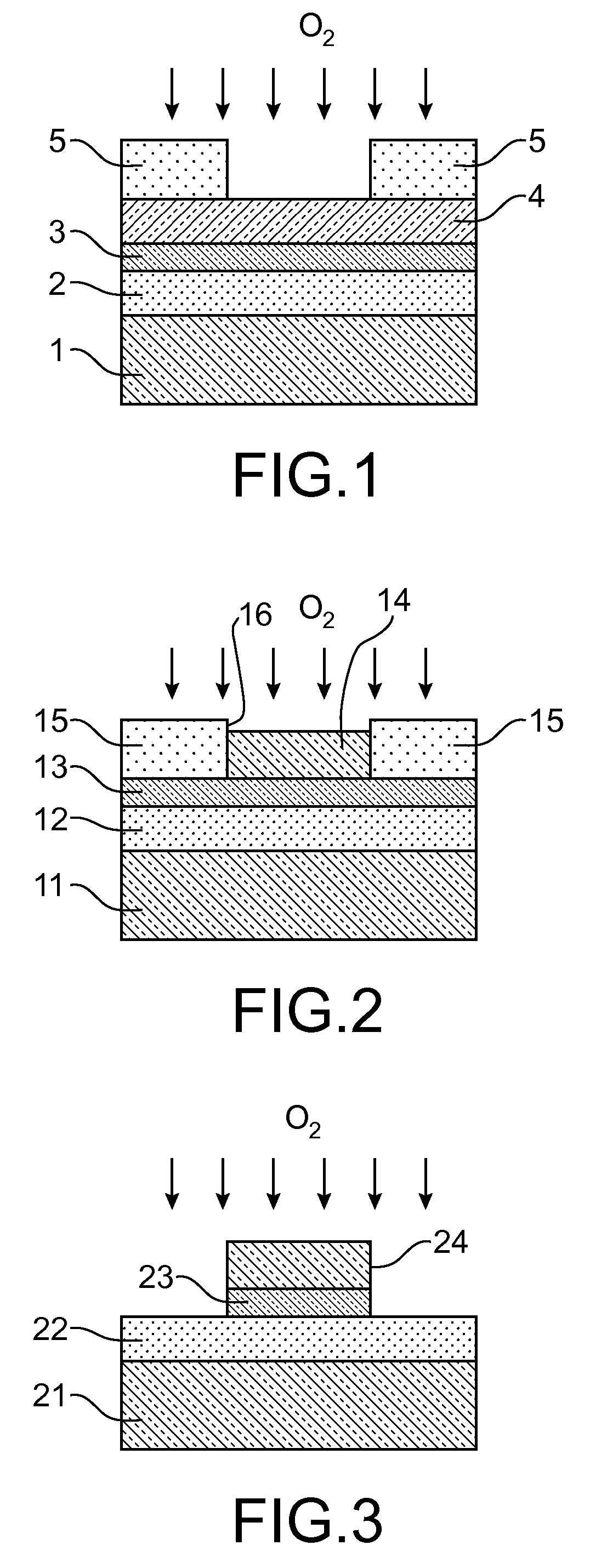
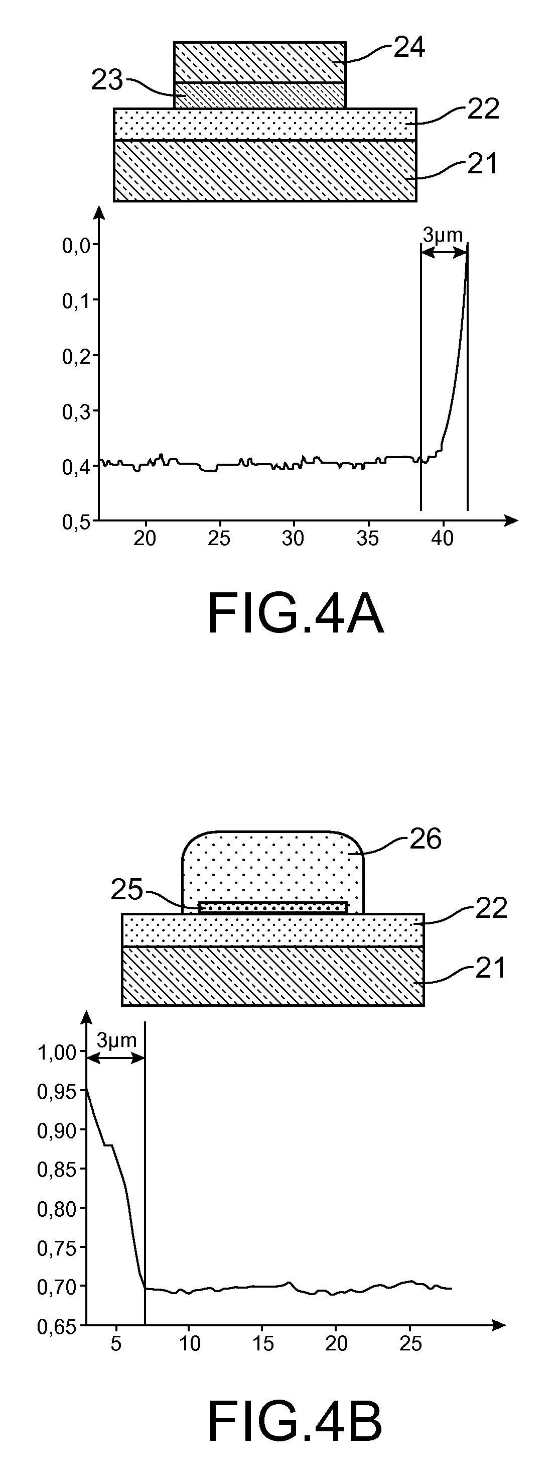
[0020]It is thus proposed to conduct localised germanium condensation on oxide fluent at low temperature. Using such oxide, in place of standard SiO2 oxide, prevents the storage of constraints during condensation and thus avoids creating structural defects.

Problems solved by technology

During condensation, boron can diffuse in the enriched oxide layer and consequently become a pollutant, as does phosphorous.

Method used


Image

  • PROCESS FOR PRODUCING LOCALISED Ge0I STRUCTURES, OBTAINED BY GERMANIUM CONDENSATION
  • PROCESS FOR PRODUCING LOCALISED Ge0I STRUCTURES, OBTAINED BY GERMANIUM CONDENSATION
  • PROCESS FOR PRODUCING LOCALISED Ge0I STRUCTURES, OBTAINED BY GERMANIUM CONDENSATION

Examples


Embodiment Construction

[0049]A particular embodiment of the invention will now be described. This embodiment is illustrated by FIGS. 5A to 5F which are views in transversal section.

[0050]FIG. 5A represents a substrate 31 made of silicon acting as support to carry out the process according to the present invention.

[0051]A layer 32 of monocrystalline SixGe1-x doped with boron or phosphorous having a concentration of germanium is formed on the substrate 31 by epitaxy, according to a method known to the man skilled in the art, resulting in a concentration of germanium corresponding from 4 to 7 m / o GeO2 in the silicon oxide which will then be formed (see FIG. 5B).

[0052]The layer 32 of SiGe is made porous by electrochemical attack in a solution of hydrofluoric acid. Sending a continuous current over a certain time period (from a few seconds to a few tens of minutes according to the preferred thickness of the porous layer, the doping rate of the SiGe layer and the nature of the dopant used) causes attack of the ...


PUM


Abstract

The invention relates to a process for making at least one GeOI structure by germanium condensation of a SiGe layer supported by a layer of silicon oxide. The layer of silicon oxide is doped with germanium, the concentration of germanium in the layer of silicon oxide being such that it lowers the flow temperature of the layer of silicon oxide below the oxidation temperature allowing germanium condensation of the SiGe layer.

Description

TECHNICAL FIELD[0001]The invention relates to a process for manufacturing localised GeOI structures, obtained by germanium condensation.PRIOR ART[0002]The race to performance (level of current, speed, . . . ) in silicon microelectronics is continually striving to miniaturise the size of transistors (Moore's law). In parallel with this miniaturisation method, introduction approaches to novel materials (for example materials with strong mobility such as germanium) and mechanical constraints (a tension constraint favours electronic transport whereas a compression constraint favours transport via holes) are under study.[0003]The base elements of C-MOS microelectronics (“Complementary Metal Oxide Semiconductor”) are N-MOS (electron conduction transistor) and P-MOS (hole conduction transistor). These two types of transistors are combined to produce logic functions (OR, AND, NOR, NAND gates, . . . ) or memory points (SRAM-6T for example). Today, all components for consumer microelectronics...

Claims


Application Information

Patent Timeline
Patent Type & Authority Applications(United States)
IPC IPC(8): H01L29/161H01L21/762
CPCH01L21/02203H01L21/02236H01L21/02255H01L29/78H01L21/31658H01L21/7624H01L29/1054H01L21/28255
Inventor DAMLENCOURT, JEAN-FRANCOISVINCENT, BENJAMIN
Owner COMMISSARIAT A LENERGIE ATOMIQUE ET AUX ENERGIES ALTERNATIVES
Why Eureka
Try Eureka