Silicon Nanoparticle Precursor

a technology of nanoparticles and precursors, applied in the field of integrated circuit fabrication, can solve the problems of many claimed materials being flammable, limited by cost and safety considerations, and many metal conductors, and achieve the effect of maximizing the packing of si nanoparticles, or minimizing the amount of liquid silane needed

Inactive Publication Date: 2010-02-25
SHARP LAB OF AMERICA INC
View PDF4 Cites 2 Cited by
  • Summary
  • Abstract
  • Description
  • Claims
  • Application Information

AI Technical Summary

Benefits of technology

[0012]The Si precursor disclosed herein minimizes, or completely eliminates the amount of a liquid silane compound needed to form a printable Si precursor, which is referred to herein as a Si nanoparticle precursor. In one aspect, the Si nanoparticle precursor is a Si-containing solution, containing Si nanoparticles, liquid silane compounds, and solvents. The major constituent of the solution is Si nanoparticles. Liquid silane compounds serves as an agent to form channels between Si nanoparticles, to form a continuous Si film after heating or light irradiation. The Si nanoparticle precursor minimizes the amount of liquid silane needed to form the proper channels by maximizing the packing of Si nanoparticles.
[0013]After deposition, the sintering of Si nanoparticles requires an elevated temperature. The sintering temperature can be reduced significantly if the connection channels are formed from liquid silane or from Ge nanoparticles. The Si nanoparticle precursor uses a designed size ratio of Si nanoparticles, to minimize the amount of liquid silane, or to reduce the use of Ge nanoparticles.

Problems solved by technology

These methods result in blanket coated films, which require patterning, typically by multiple photolithography and etch steps.
However, such a practice is limited by considerations of cost and safety.
It is known that many of the claimed materials are flammable and in some cases, such as germanium-containing precursor, can also be toxic.
Although a safe operation can be maintained in an enclosure using sophisticated safety precautions, the manufacturing costs associated with flammable materials are high.
The end result may be that the cost of a so-called “low-cost” Si printing process will become too high for actual practice.
However, none of the above-mentioned methods provide an analysis of the amount or percentage of Si-containing compound required to form silicon films.

Method used


Image

  • Silicon Nanoparticle Precursor
  • Silicon Nanoparticle Precursor
  • Silicon Nanoparticle Precursor

Examples


example 1

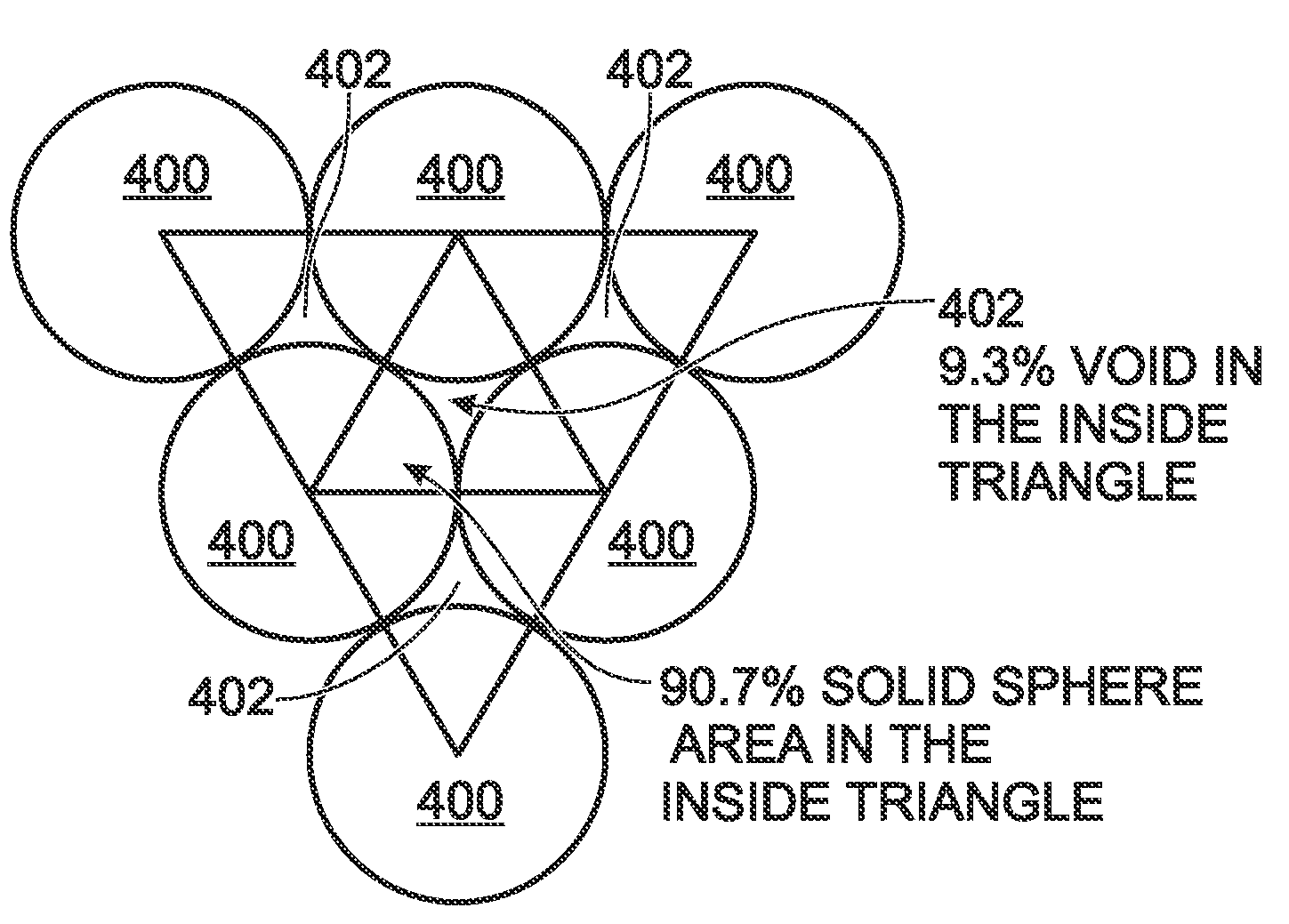
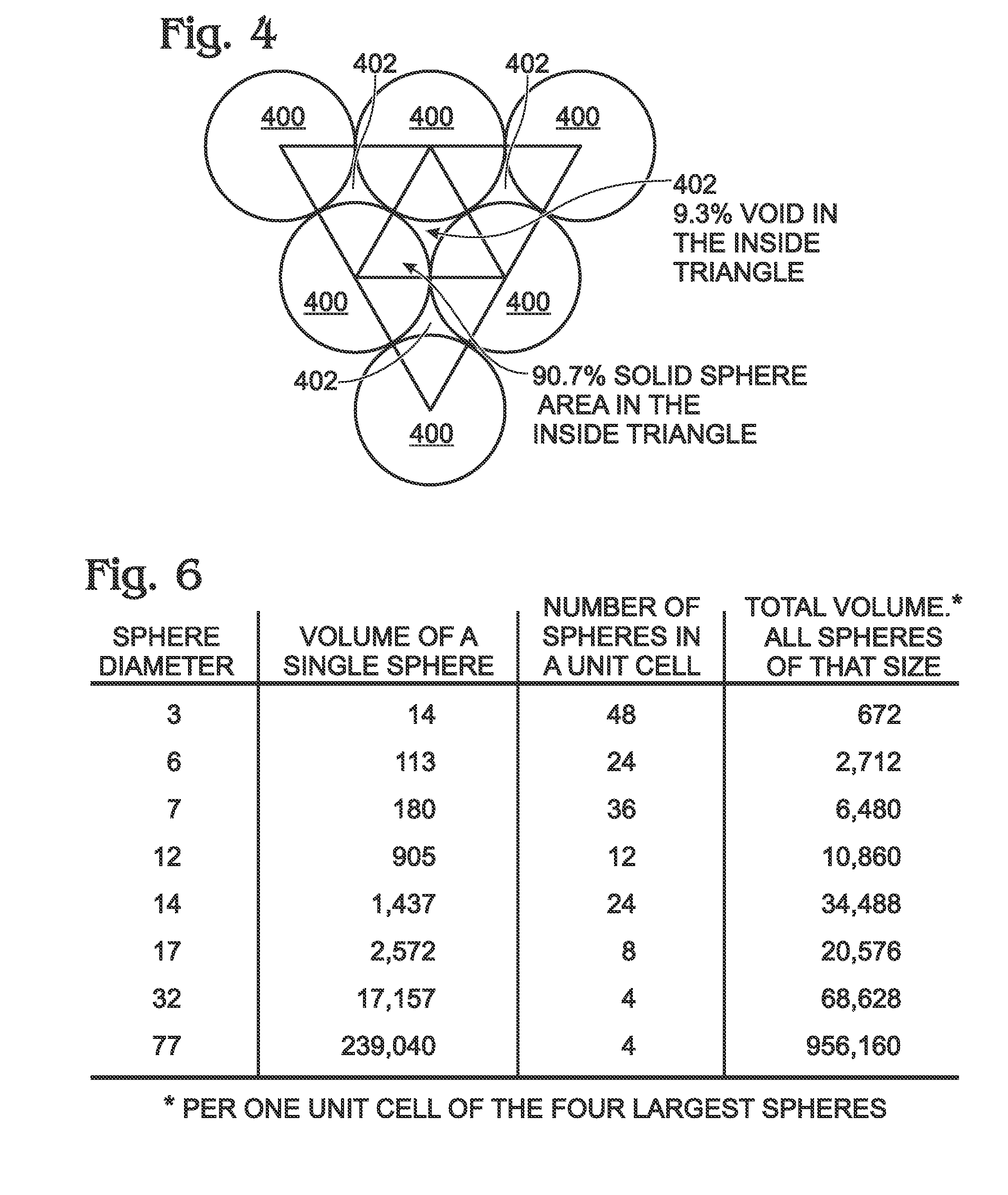
[0040]Mix Si particles in a size ratio of around 77:32:17 or 77:32:17:D, where D=12˜14. As an example, the sizes of the particles can be: 39 nm, 16 nm, and 8˜9 nm. The ratio of wt. % is: 956 gm (39 nm):69 gm (16 nm):21 gm (8˜9 nm). Since the nanoparticle material is silicon in this example, the weight ratio is directly proportional to the volume ratio as shown in the table of FIG. 6.

[0041]Add a liquid silane compound dissolved in an organic solvent, with volume ratio of 5˜15% of the total volume. When liquid silane is added, Si nanoparticles are arranged in two or more classes. For example, 77:32, 77:32:17, or more combinations.

example 2

[0042]Mix Si nanoparticles with Ge nanoparticles, in a size ratio of 77 (Si):32 (Ge) or 77 (Si):32 (Si):17 (Ge). There are multiple ways to form the mixture. The weight ratio is adjusted according to the density of silicon and germanium, and follows the volume ratio of the table in FIG. 6.

[0043]Annealing can be performed in an inert environment using a furnace, laser, rapid thermal annealing (RTA), or by flash lamp annealing method.

[0044]Although the addition of liquid silane or Ge can help form conduction channels among Si nanoparticles at a much lower temperature, it is also possible to form Si films by arranging the nanoparticles in proper size ratio without the addition of liquid silane or Ge. Si nanoparticles with size ratio of 77:32:17 or 77:32:1.7:12˜14 can be mixed in a dispersion solution and applied onto substrates. Sintering is then performed using one of the above-mentioned annealing methods.

[0045]FIG. 7 is a flowchart illustrating a method for forming a Si nanoparticle ...


PUM

PropertyMeasurementUnit
temperatureaaaaaaaaaa
sizesaaaaaaaaaa
sizesaaaaaaaaaa

Abstract

A Si nanoparticle precursor, precursor fabrication process, and precursor deposition process are presented. The method for forming a silicon (Si) nanoparticle precursor provides a plurality of nanoparticle classes, including at least one Si nanoparticle class. The nanoparticles in each nanoparticle class are defined as having a predetermined diameter. A predetermined amount of each nanoparticle class is measured and combined. For example, a first Si nanoparticle class may be provided having a largest diameter and a second Si nanoparticle class having a second-largest diameter equal to about (0.43)×(the largest diameter). As another example, Si nanoparticle classes may foe provided having a diameter ratio of about 77:32:17.

Description

BACKGROUND OF THE INVENTION[0001]1. Field of the Invention[0002]This invention generally relates to integrated circuit (IC) fabrication and, more particularly, to a silicon (Si) nanoparticle precursor that can be sintered at low temperatures to form Si thin-films.[0003]2. Description of the Related Art[0004]Silicon, thin-film transistors (TFTs) are commonly used as active-matrix devices in flat-panel displays. Due to severe competition within the display industry, cost reduction in the fabrication process is always an essential goal in the design of new products. Conventionally, a TFT fabrication process uses several chemical vapor deposition (CVD) and / or sputtering steps to deposit semiconductor, insulator, and conductor materials, which require vacuum systems, gas delivery, and control units. These methods result in blanket coated films, which require patterning, typically by multiple photolithography and etch steps. The cost of these processes could be reduced significantly if th...

Claims


Application Information

Patent Timeline
Patent Type & Authority Applications(United States)
IPC IPC(8): B05D5/12H01B1/04
CPCC01B33/021
Inventor MAA, JER-SHENHERMAN, GREGORY S.VOUTSAS, APOSTOLOS T.
Owner SHARP LAB OF AMERICA INC
Why Eureka
Try Eureka