
Substrate processing method

a processing method and substrate technology, applied in the field of substrate processing methods, can solve the problems of limited photolithography mass production limit, and achieve the effects of reducing the opening width of the mask layer and the opening of the intermediate layer

Active Publication Date: 2010-02-25
TOKYO ELECTRON LTD
View PDF2 Cites 9 Cited by
  • Summary
  • Abstract
  • Description
  • Claims
  • Application Information

AI Technical Summary

Benefits of technology

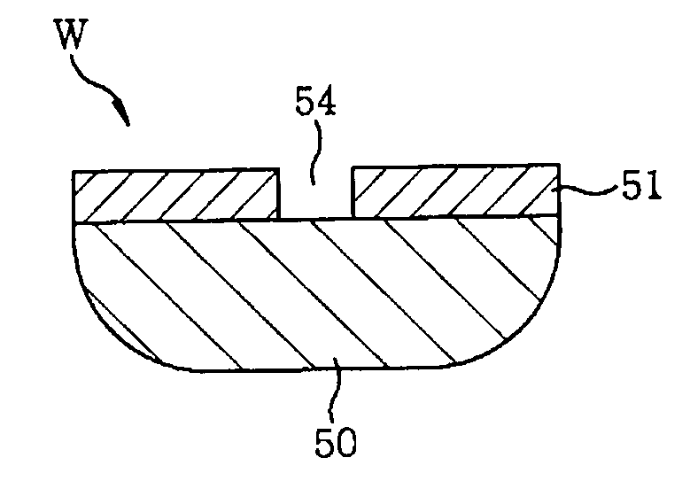
The present invention provides a substrate processing method for forming an opening of a size that satisfies a demand for miniaturization of semiconductor devices in a mask film or an intermediate film on a substrate. The method involves depositing a deposit on the sidewall surface of the opening of the mask layer using a gas mixture of depositive gas and SF6 gas, and then etching the intermediate layer to form an opening with the same width as the reduced opening of the mask layer. The method can reduce the opening width of the mask layer by depositing deposits and etching the intermediate layer, and can provide an opening pattern with a reduced opening width that satisfies the demand for miniaturization of semiconductor devices. The method can also reduce the roughness and abrasion of the substrate surface, and can be carried out within minimum processing time. The intermediate layer to be etched is the BARC film stacked below the mask layer, which allows for the formation of an opening with the same size as the mask layer.

Problems solved by technology

Although the minimum size of the pattern in the photoresist film is restricted by a minimum size that can be developed by photolithography, the minimum size that can be mass-produced by photolithography is limited due to variation of a focal length or the like.

Method used


Image

  • Substrate processing method
  • Substrate processing method
  • Substrate processing method

Examples


Embodiment Construction

[0030]The embodiments of the present invention will be described with reference to the accompanying drawings which form a part hereof.

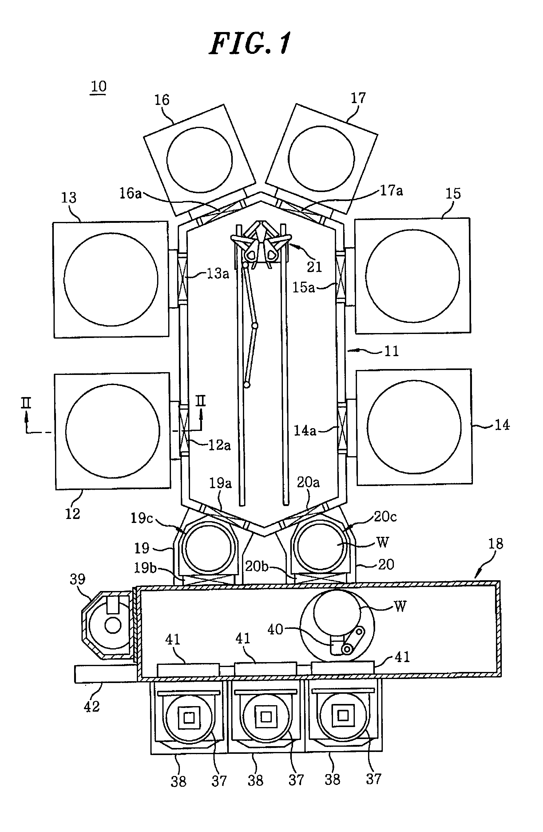
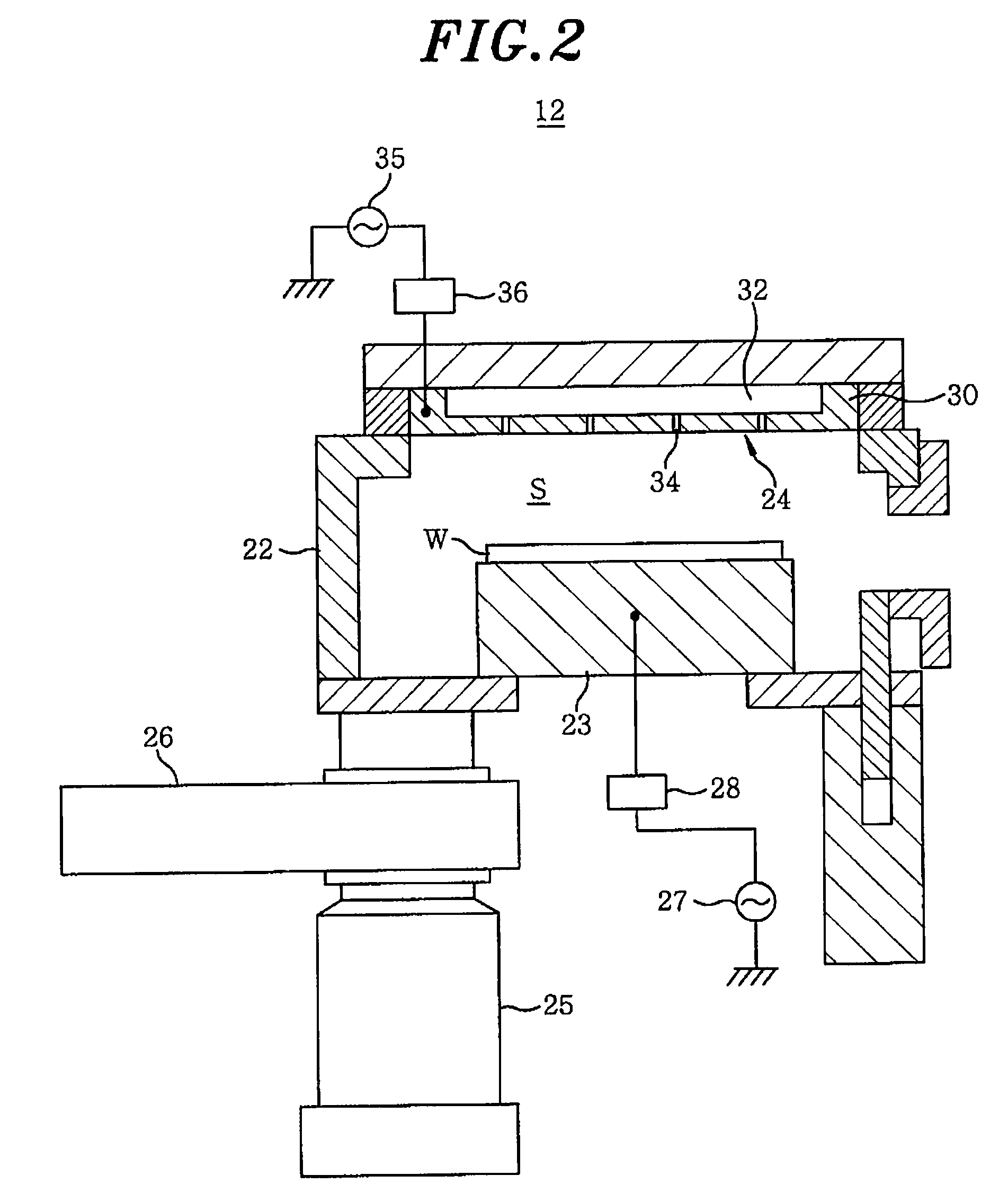
[0031]First of all, a substrate processing system for performing a substrate processing method in accordance with an embodiment of the present invention will be described. The substrate processing system includes a plurality of process modules configured to perform etching or ashing on a substrate, e.g., a semiconductor wafer W, by using a plasma.

[0032]FIG. 1 is a top view schematically showing the configuration of the substrate processing system for performing the substrate processing method in accordance with an embodiment of the present invention.

[0033]Referring to FIG. 1, a substrate processing system 10 includes a transfer module 11 of a hexagonal shape seen from above, two process modules 12 and 13 connected to one side of the transfer module 11, and two process modules 14 and 15 connected to the other side of the transfer module 11 so as to fac...


PUM

PropertyMeasurementUnit
bias poweraaaaaaaaaa
pressureaaaaaaaaaa
pressureaaaaaaaaaa

Abstract

A substrate processing method for processing a substrate, on which a processing target layer, an intermediate layer, and a mask layer having an opening to expose a part of the intermediate layer are stacked in this order, includes a shrink etching step. In the shrink etching step, an opening width of the opening of the mask layer is reduced by depositing deposits on a sidewall surface thereof by a plasma generated from a gaseous mixture of depositive gas expressed by a general formula CxHyFz (x, y and z being positive integers) and SF6 gas. Also, there is formed in the intermediate layer an opening having an opening width corresponding to the reduced opening width of the opening of the mask layer by etching the intermediate layer.

Description

FIELD OF THE INVENTION[0001]The present invention relates to a substrate processing method; and, more particularly, to a substrate processing method for processing a substrate on which a processing target layer, an intermediate layer and a mask layer are stacked in this order.BACKGROUND OF THE INVENTION[0002]There is known a wafer for a semiconductor device in which an oxide film containing impurities, e.g., a Tetra Ethyl Ortho Silicate (TEOS) film, formed by a CVD process or the like, a conductive film such as a TiN film, a bottom anti-reflection coating (BARC) film and a photoresist film are stacked in this order on a silicon base member (see, e.g., Patent Document 1). The photoresist film is formed in a predetermined pattern by photolithography, and serves as a mask layer when the BARC film and the conductive film are etched.[0003]A recent trend toward miniaturization of semiconductor devices requires a finer circuit pattern on a wafer surface. In order to form a finer circuit pa...

Claims


Application Information

Patent Timeline
Patent Type & Authority Applications(United States)
IPC IPC(8): H01L21/3065
CPCH01L21/0206H01L21/0337H01L21/31144H01L21/31116H01L21/31138H01L21/0338
Inventor SONE, TAKASHINISHIMURA, ELLCHL
Owner TOKYO ELECTRON LTD
Learn More