LED Structure

a technology of led structures and led components, applied in the direction of semiconductor/solid-state device manufacturing, electrical apparatus, semiconductor devices, etc., can solve the problems of weak productivity, high manufacturing cost, and inability to connect two led structures without sub-mounts, and achieve the effect of improving elaborateness

Inactive Publication Date: 2010-03-11
HELIO OPTOELECTRONICS
View PDF4 Cites 73 Cited by
  • Summary
  • Abstract
  • Description
  • Claims
  • Application Information

AI Technical Summary

Benefits of technology

[0011]The primary objective of the present invention is to provide a novel LED structure that remedies the defects of the conventional products while facilitating interconnection between LEDs and easy manufacture of an LED single-structure that has improved elaborateness and is operable in a high-voltage environment, thus being more utility.

Problems solved by technology

Although the structure of U.S. Pat. No. 6,853,011 is applicable to flip-chip structures, it would be impossible to connect two of the LED structures without assistance of submounts.
Besides, complexity of the flip-chip process could be significantly increased because there are numerous chips to be processed.
On the other hand, while the structure of U.S. Pat. No. 6,998,642 enables the electrical connection between LEDs, metal-to-metal adherence where such electrical connection relies could be only achieved through a complex process, resulting in problems related to weak productivity and high manufacturing costs.
Moreover, since the nonconductive layer is located at the boundary between the LEDs, the metal connection trace could only connect two electrically conducting plates and it would still be impossible to achieve a circuit layout with further complexity if no submounts are provided.
Although all relevant manufactures have saved no efforts to solve the aforementioned problems, an applicable approach has not been developed.
It is still a challenge for the manufacturers to provide an appropriate structure to all related products with the attempt solving the aforementioned problems.

Method used


Image

  • LED Structure
  • LED Structure
  • LED Structure

Examples


first preferred embodiment

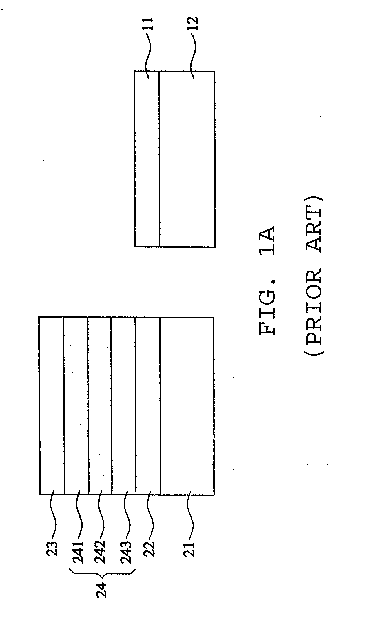
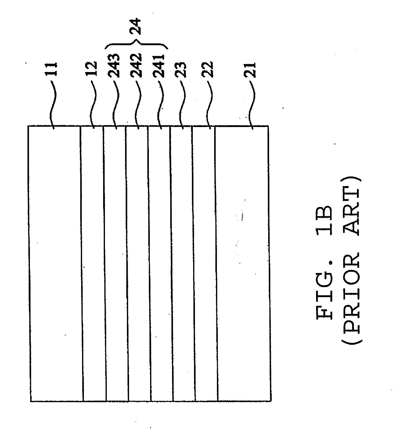
[0064]Please refer to FIGS. 1A, 1B and 1C for a schematic drawing showing a conventional first substrate 21 and a pre-processing LED structure 10 to be assembled together, a schematic drawing showing the first substrate 21 and the pre-processing LED structure 10 assembled together, and a schematic drawing according to FIG. 1B showing a temporary substrate 11 and an etch-stop layer 12 removed therefrom.

[0065]Conventionally, the pre-processing LED structure 10 that will later receive unit division, isolation layer formation and electrically conducting plate installation is formed on a wafer through a semiconductor process. However, since being undesirably thick and opaque and thus unfavorable to practical applications of the LED structure, the wafer has to be removed later. In other words, the wafer is a substrate for temporary use during the process for constructing the LED structure, and thus is herein referred to as the temporary substrate 11.

[0066]Among the known methods for remov...

second preferred embodiment

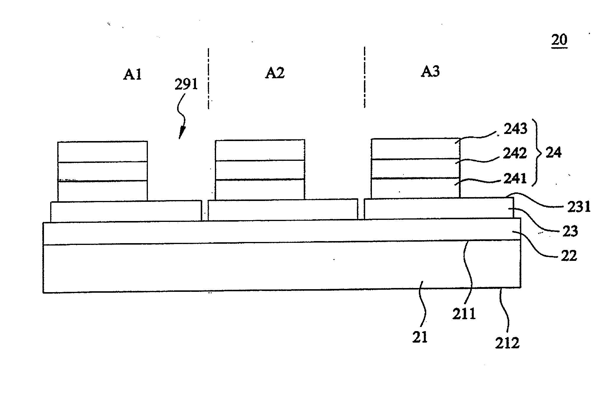
[0085]Please refer to FIGS. 7 to 9 for the LED structure 30 according to another embodiment of the present invention. The LED structure 30 includes a first substrate 21, an adhering layer 22, at least two first ohmic contact layers 23, at least two epi-layers 24, a second isolation layer 31, at least two fifth electrically conducting plates 32, and at least two sixth electrically conducting plates 33.

[0086]The LED structure 30 of the present embodiment may be also made through the process for the first embodiment as shown in FIGS. 1A to 1C. Similarly, the first substrate 21 with the adhering layer 22 attached thereto is bound with the pre-processing LEDs 28. Then the temporary substrate 11 and the etch-stop layer 12 are removed therefrom by etching so as to obtain the pre-unit-division LED structure 30.

[0087]The first substrate 21 has a first surface 211 and a second surface212 and primarily serves to support the whole LED structure 30. The first substrate 21 may be a monocrystal su...


PUM


Abstract

An LED structure includes a first substrate; an adhering layer formed on the first substrate; first ohmic contact layers formed on the adhering layer; epi-layers formed on the first ohmic contact layers; a first isolation layer covering the first ohmic contact layers and the epi-layers at exposed surfaces thereof; and first electrically conducting plates and second electrically conducting plates, both formed in the first isolation layer and electrically connected to the first ohmic contact layers and the epi-layers, respectively. The first trenches or the second trenches allow the LED structure to facilitate complex serial/parallel connection so as to achieve easy and various applications of the LED structure in the form of single structures under a high-voltage environment.

Description

BACKGROUND OF THE INVENTION[0001]1. Technical Field[0002]The present invention relates to LED structures, and more particularly, to a high-power LED structure operable in a high-voltage environment.[0003]2. Description of Related Art[0004]U.S. Pat. No. 6,853,011 has disclosed a light emitting epi-layer structure containing a temporary substrate of absorption light type on one side while the other side thereof is then adhered to a transparent substrate of light absorption free by BCB bonding layer. After the temporary substrate is removed, the resulted light emitting structure is then patterned to form a connection channel to connect the first ohmic contact electrode and form an isolation trench to separate the active layer of the light emitting structure into two parts. Thereafter, a second ohmic contact electrode on the cladding layer and a bonding metal layer filled in the first channel and on second ohmic contact electrode are successively formed. The resulted LED structure is he...

Claims


Application Information

Patent Timeline
Patent Type & Authority Applications(United States)
IPC IPC(8): H01L33/00H01L33/38H01L33/62
CPCH01L27/156H01L33/385H01L33/44H01L2224/16225H01L33/62H01L24/05H01L24/06H01L2224/0401H01L2224/05001H01L2224/05009H01L2224/0557H01L2224/05571H01L2224/06102H01L2224/16238H01L2224/1703H01L2924/00014H01L2224/05599H01L2224/05099
Inventor SHEI, SHIH-CHANGCHEN, MING-HUNGWEN, SHIH-YILEE, CHUN-CHE
Owner HELIO OPTOELECTRONICS
Why Eureka
Try Eureka