Clock control of state storage circuitry

a state storage circuit and clock control technology, applied in the direction of logic circuits, information storage, electronic circuit testing, etc., can solve the problems of slow propagation of data signals into the master stage, increase the clock to output delay, etc., to increase the complexity of clock signal generating circuitry, increase the maximum speed of state storage circuitry, and operate faster

Active Publication Date: 2010-03-11
ARM LTD
View PDF7 Cites 3 Cited by
  • Summary
  • Abstract
  • Description
  • Claims
  • Application Information

AI Technical Summary

Benefits of technology

[0013]The invention realises that the functional path input through the tristate logic circuitry can be tristated as needed during scan by holding its clock signals at appropriate values. This has the result that the tristate logic circuitry need no longer include gates switched by the scan enable signal. This makes the tristate logic circuitry faster to operate and increases the maximum speed of the state storage circuitry. In practice the technique can be considered as moving control of the tristating of the tristate logic circuitry from the tristate logic circuitry itself into the clock signal generating circuitry. This increases the complexity of the clock signal generating circuitry, but the advantage in the increased speed of the tristate logic circuitry more than compensates.
[0014]It will be appreciated that the tristate logic circuitry could have a variety of different forms. It may be responsive to multiple data input signals, e.g. it could provide logic functions such as AND, OR, etc. However, a simple, fast and effective use of the present technique is when the tristate logic circuitry is tristate inverter circuitry responsive to the third clock signal and the fourth clock signal to drive the storage signal to an inverted value of a functional input signal. State storage circuitry having this functionality is common within integrated circuits and improvements in the speed of such elements are strongly advantageous.
[0015]In some embodiments the tristate inverter circuitry can comprise a stack of two P-type inverter circuitry transistors and two N-type inverter circuitry transistors switched by the functional input signal and the third and fourth clock signals. This is a compact and efficient arrangement.
[0019]The tristate invertor within the master-slave latch may be switched by the first clock signal and the second clock signal. The first clock signal and the second clock signal are no longer being used to tristate the tristate logic circuitry and accordingly the clock to output delay can be reduced whilst not at the same time adversely directly impacting the setup time as the tristate logic circuitry is controlled by its own clocks.
[0024]Whilst the relationship between the different clock signals could vary and will typically include some time lag, it is advantageously simple when the second clock signal is a complement of the first clock signal and the fourth clock signal is a complement of the third clock signal.

Problems solved by technology

A first problem is that the functional data path into the latch is via a stack of six gates, namely three P-type gates and three N-type gates.
This slows propagation of a data signal into the master stage.
Thus, whilst it may be desired to delay the time at which the six gate stack becomes tristated to permit a greater time for the master stage to properly capture the data value, this has a consequence of also increasing the clock to output delay.

Method used


Image

  • Clock control of state storage circuitry
  • Clock control of state storage circuitry
  • Clock control of state storage circuitry

Examples


Embodiment Construction

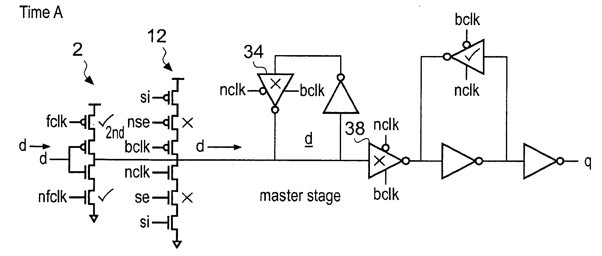
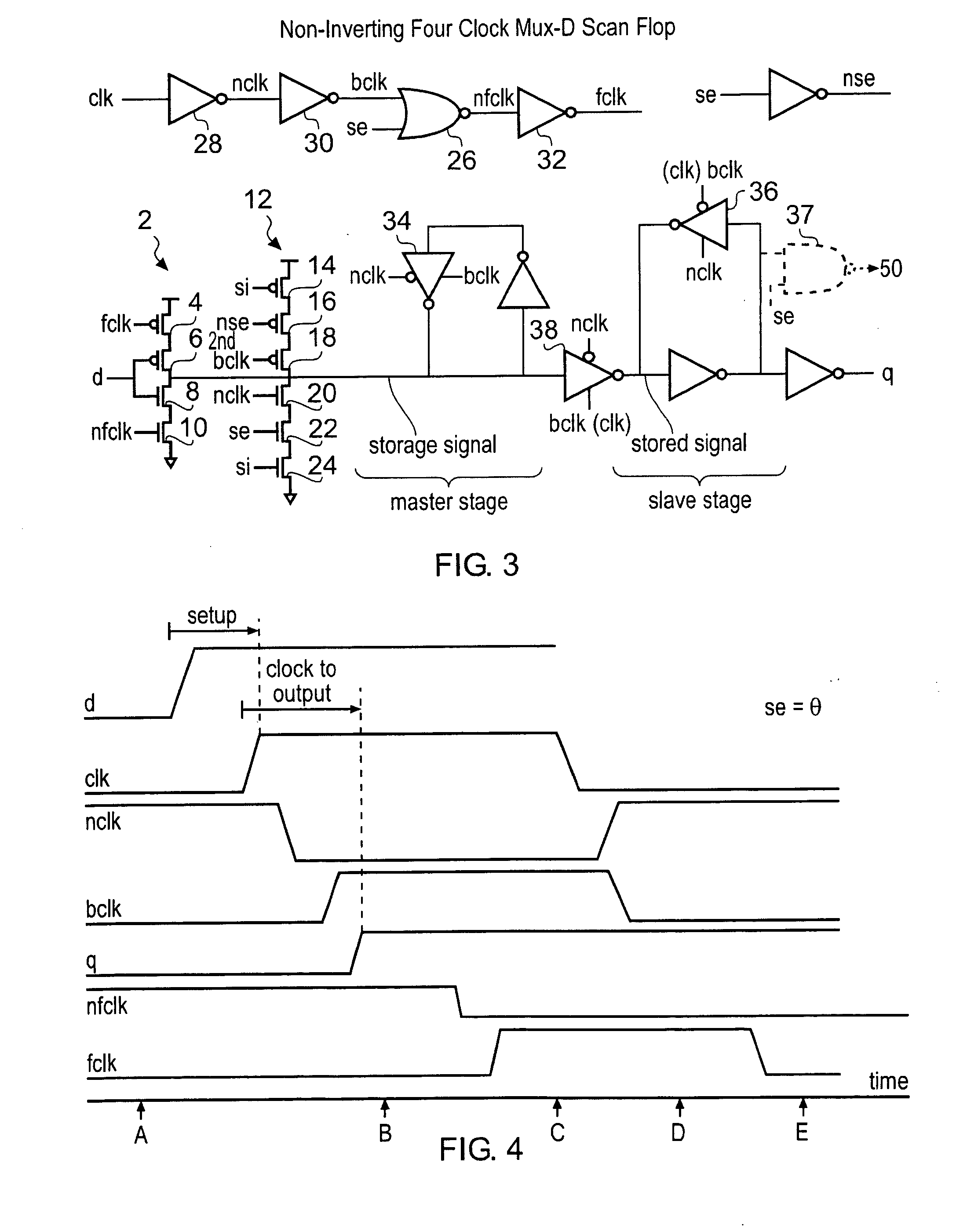
[0037]FIG. 3 shows tristate logic circuitry in the form of tristate inverter circuitry 2 comprising two P-type gates 4, 6 and two N-type gates 8, 10. The output from this tristate inverting circuitry 2 drives the storage signal which is applied to the master stage of the state storage circuitry. Tristate scan signal insertion circuitry 12 comprises three P-type gates 14, 16, 18 and three N-type gates 20, 22, 24. The tristate scan signal insertion circuitry 12 drives the storage signal during scan mode.

[0038]In functional mode the scan enable signal se is not asserted (low) and accordingly gates 22 and 16 are switched off and the tristate scan signal insertion circuitry 12 is tristated and not driving the storage signal. During the scan mode the tristate scan signal insertion circuitry 12 does drive the storage signal and in this case the clock signals to the gates 4 and 10 respectively comprising the fourth clock signal fclk and the third clock signal nfclk are held at fixed values ...


PUM


Abstract

State storage circuitry is described comprising a master-slave latch having tristate inverter circuitry 2 at its functional input and tristate scan signal insertion circuitry 12 for inserting scan data. The tristate scan signal insertion circuitry 12 is controlled by a first clock signal nclk and a second clock signal bclk. The tristate inverter circuitry 2 is controlled by a third clock signal nfclk and a fourth clock signal flck. The clock generating circuitry holds the third and fourth clock signals at fixed values which tristate the tristate inverter circuitry 2 when in scan mode. This moves scan control logic out of the function path comprising the tristate inverter circuitry into the clock control circuitry.

Description

BACKGROUND OF THE INVENTION[0001]1. Field of the Invention[0002]This invention relates to the field of state storage circuitry, including different types of latches, flip-flops, registers etc. More particularly, this invention relates to the control of such state storage circuitry with clock signals.[0003]2. Description of the Prior Art[0004]FIG. 1 of the accompanying drawings illustrates a known inverting mux-D scan flop built using CMOS circuitry. The functional data signal d is applied to a P-type gate and a N-type gate within a stack comprising three P-type gates and three N-type gates. This stack also includes two gates switched by the scan enable signal se and the complement of the scan enable signal nse. The final two transistors within the stack are switched by the complement nclk of the input clock clk to the clock tree illustrated as well as a buffered clock bclk generated from clock nclk. When scan enable is not asserted, the gates controlled by the scan enable signal se ...

Claims


Application Information

Patent Timeline
Patent Type & Authority Applications(United States)
IPC IPC(8): H03K19/096H03K3/289H03K3/037
CPCG11C7/1078G11C19/00G11C7/1087
Inventor KVINTA, STEPHEN ANDREWFREDERICK, MARLIN WAYNEHUANG, CHIH-WEI
Owner ARM LTD
Why Eureka
Try Eureka