Amplification circuit

a technology of amplifiers and circuits, applied in amplifiers, amplifiers with semiconductor devices/discharge tubes, amplifiers, etc., can solve problems such as increasing attenuation, and achieve the effect of wide dynamic range and good signal quality

Active Publication Date: 2010-03-11
RENESAS ELECTRONICS CORP
View PDF4 Cites 30 Cited by
  • Summary
  • Abstract
  • Description
  • Claims
  • Application Information

AI Technical Summary

Benefits of technology

[0057]According to the present invention, the impedance converting circuits are connected to each other by the switching circuit of the first type having the signal cutting-off function, and the switching circuit of the second type is connected to the signal path branched from the input side of the switching circuit of the first type, or the impedance converting circuits that are connected to each other by the switching circuit of the first type that have the signal cutting-off function are connected to the switching circuit of the second type that have the signal cutting-off function which is connected between the output and input sides of the switching circuit of the first type. With this arrangement, the amplifying circuit is operable in a wide frequency band.
[0058]Since the switching circuits connected in series to the amplifiers have the signal attenuating function, the amplifying circuit provide a wide dynamic range when it is operated under a low voltage.
[0059]Since the amplifying circuit according to the present in

Problems solved by technology

By increasing the number of attenuating capacitors by rendering other transistors conductiv

Method used


Image

  • Amplification circuit
  • Amplification circuit
  • Amplification circuit

Examples


exemplary embodiment 2

[0105]FIG. 5 is a circuit diagram of a second exemplary embodiment of the present invention. In the present exemplary embodiment, amplifiers 1011, 1012 shown in FIG. 4 are replaced with single amplifier 101. Amplifier 101 includes inductor L11 and n-type MOSFETs Q11, Q12. MOSFET Q12 has a source electrode connected to ground, a gate electrode supplied with an RF signal in a high frequency band, and a drain electrode connected to output terminal OUT.

[0106]MOSFET Q11 has a source electrode grounded, a gate electrode supplied with an RF signal in a low frequency band, and a drain electrode connected to output terminal OUT. Inductor L11 is connected as a load on MOSFETs Q11, Q12 between power supply terminal Vdd and the drains of the respective transistors. The input RF signals are controlled by control signal generating circuit 102 such that only their desired frequency bands are propagated. Therefore, only one of the MOSFETs of amplifier 101 which is connected to the path in the desir...

exemplary embodiment 1

[0109]FIG. 7 is a circuit diagram of a third exemplary embodiment of the present invention. The circuit according to the present exemplary embodiment comprises two circuits according to the second exemplary embodiment which are connected parallel to each other. In FIG. 7, IN1, IN2 represent input terminals to which an RF signal is input, MT11, MT21; MT12, MT22 matching circuits, C11, C21; C12, C22 capacitors, L11, L21; L12, L22 inductors, Q11, Q21; Q12, Q22 n-type MOSFETs, and Q111, Q121; Q122, Q122 n-type MOSFETs having inductor L11 as a common load. Control signal generating circuit 102 selectively renders either one of MOSFETs Q11, Q21; Q12, Q22 to select a signal path.

[0110]If a plurality of frequency bands to be handled are largely different from each other, it is difficult to separate a high frequency band and a low frequency band from each other with a single signal path. Depending on the communication scheme, it may be necessary to connect a filter for removing interfering w...

exemplary embodiment 4

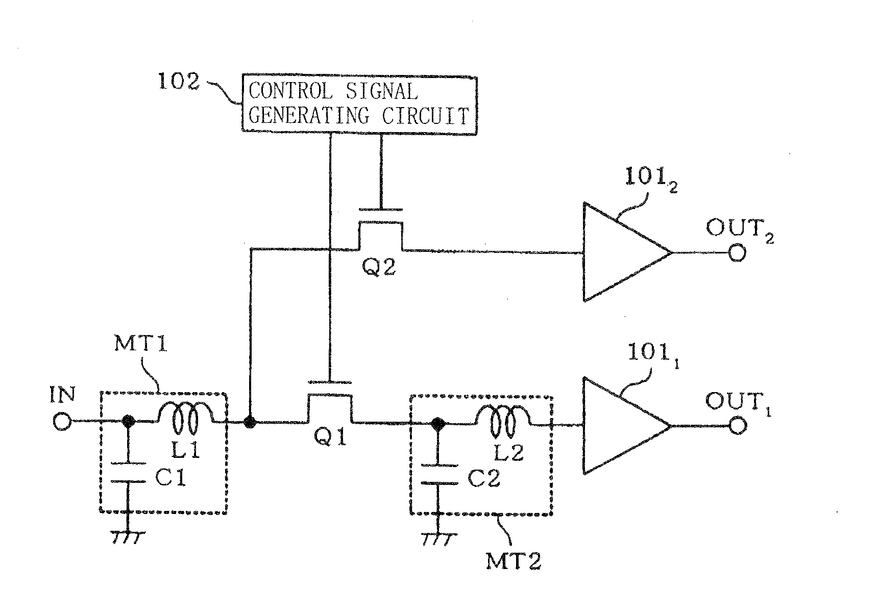
[0112]FIG. 8 is a circuit diagram of a fourth exemplary embodiment of the present invention. The circuit according to the present exemplary embodiment is different from the amplifying circuit according to the first exemplary embodiment in that it includes another matching circuit added to the RF signal path for the low frequency band and additionally includes an RF signal path for an intermediate frequency band. In FIG. 8, IN represents an input terminal to which an RF signal is input, OUT1 through OUT3 are an output terminal, MT1 through MT2 are matching circuits, C1 through C3 are capacitors, L1 through L3 are inductors, Q1 through Q4 are switching n-type MOSFETs, 1011 is an amplifier which operates in a low frequency band, 1012 an amplifier which operates in a high frequency band, 1013 is an amplifier which operates in an intermediate frequency band, and 102 is a control signal generating circuit for outputting control signals to MOSFETs Q1 through Q4 for selecting signal paths.

[...


PUM


Abstract

The present invention is aimed at realizing an amplifying circuit whose chip size is prevented from being significantly increased even if the number of compatible frequencies increases, and which has a wide dynamic range when it operates under a low voltage. The amplifying circuit includes a plurality of impedance converting circuits connected to each other by a switching circuit of a first type having a signal cutting-off function, a switching circuit of a second type connected to a path branched from an input side of the switching circuit of the first type, the switching circuit of the second type having a signal cutting-off function, amplifiers connected respectively to an output side of one of the impedance converting circuits in a final stage and to an output side of the switching circuit of the second type, and a control signal generating circuit for controlling connection/disconnection between said switching circuit of the first type and said switching circuit of the second type; wherein either one of the paths is selected to input a signal to one of the amplifiers.

Description

TECHNICAL FIELD[0001]The present invention relates to an amplifier which has a wide dynamic range when it operates under a low voltage and which operates in a wide frequency range.BACKGROUND ART[0002]The Global system for Mobile Communications (GSM) and the Digital Cellular system (DCS) for use in the second-generation cellular phones according to the present global mainstream cellular phone system have already employed four radio frequency bands of 800, 900, 1800, 1900 MHz in order to provide a wide user area. In the future, as second-generation cellular phones shift to third-generation cellular phones based on Enhanced Data GSM Environment (EDGE), CDMA (Code Division Multiple Access), and Wideband CDMA (WCDMA) systems, dual terminals that are individually capable of using second- and third-generation services will be put into service, which will require that cellular phones be compatible with 1.7 GHz and 2 GHz bands in addition to the above four bands.[0003]The study of high-speed...

Claims


Application Information

Patent Timeline
IPC IPC(8): H03F3/68
CPCH03F1/42H03F1/565H03F3/68H03F3/195H03F3/005
Inventor MAEDA, TADASHI
Owner RENESAS ELECTRONICS CORP
Why Eureka
Try Eureka