Novel fused polycyclic aromatic compound, process for producing the same, and use thereof

Active Publication Date: 2010-03-18
NIPPON KAYAKU CO LTD
View PDF4 Cites 40 Cited by
  • Summary
  • Abstract
  • Description
  • Claims
  • Application Information

AI Technical Summary

Benefits of technology

[0084]Since the on/off current ratio is not less than 105, a ratio between an on current and an off current is large, which causes a current to be large in an on state in which the largest current flows between a source and a drain, thereby resulting in that a high-performance organic semiconductor device can be provided.
[0085]Moreover, in the organic semiconductor device of the present invention, it is preferable that

Problems solved by technology

Further, in organic FET devices, the electron field-effect mobility directly affects switching speed and performances of a device to be driven.
Generally, such organic semiconductors have a low electron field-effect mobility compared with silicon semiconductors, and this prevents practical use of the organic semiconductors.
However, the increase of the fused-ring number makes it difficult to dissolve the material of a semiconductor layer, or causes a decreas

Method used


Image

  • Novel fused polycyclic aromatic compound, process for producing the same, and use thereof
  • Novel fused polycyclic aromatic compound, process for producing the same, and use thereof
  • Novel fused polycyclic aromatic compound, process for producing the same, and use thereof

Examples


embodiment 1

[0109]In order to obtain (a) a compound including: a BXBX skeleton further having an aromatic ring(s) located outside the BXBX skeleton, or (b) a compound including a BXBX skeleton in which a benzene ring is substituted with a heterocyclic ring, the inventors of the present invention diligently worked to find how to obtain a compound 1 by use of a reaction represented by the following Reaction Formula (1):

However, it was quite difficult to obtain a compound 2, which is a source material of the compound 1, and a compound 3, which is a source material for synthesizing the compound 2. The compound 3 is represented by the following General Formula (18):

[0110]There is a compound 2a having a similar structure to the compound 2 and represented by General Formula (19):

The compound 2a can be obtained by reacting compounds 3a with each other, the compound 3a being represented by the following General Formula (20):

The inventors synthesized the compound 3a by use of multistage reaction represen...

embodiment 2

[0147]Another embodiment of the present invention will be explained as follows. A production method of the present embodiment is to produce a compound represented by the following General Formula (17):

and the method of the present embodiment includes the steps of: (i) reacting compounds represented by General Formula (7) with each other so as to obtain a compound represented by General Formula (16):

the compounds represented by General Formula (7) being obtained by the production method according to Embodiment 1; and (ii) after the step (i), reacting the obtained compound represented by General Formula (16) with iodine.

[0148]In both of the formulae, X18 and X19 are independently a chalcogen atom; each Ar independently has a structure selected from the group consisting of the following chemical structures (a) through (c):

[0149](a) a chemical structure having at least one benzene ring to fuse, in which a hydrogen atom may be substituted with an atom or a functional group selected from ...

embodiment 3

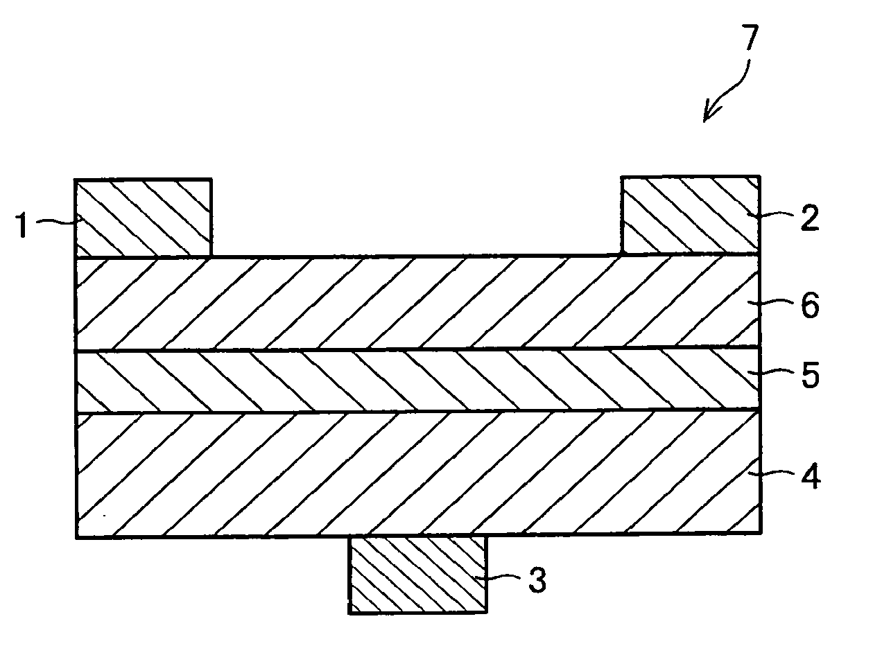
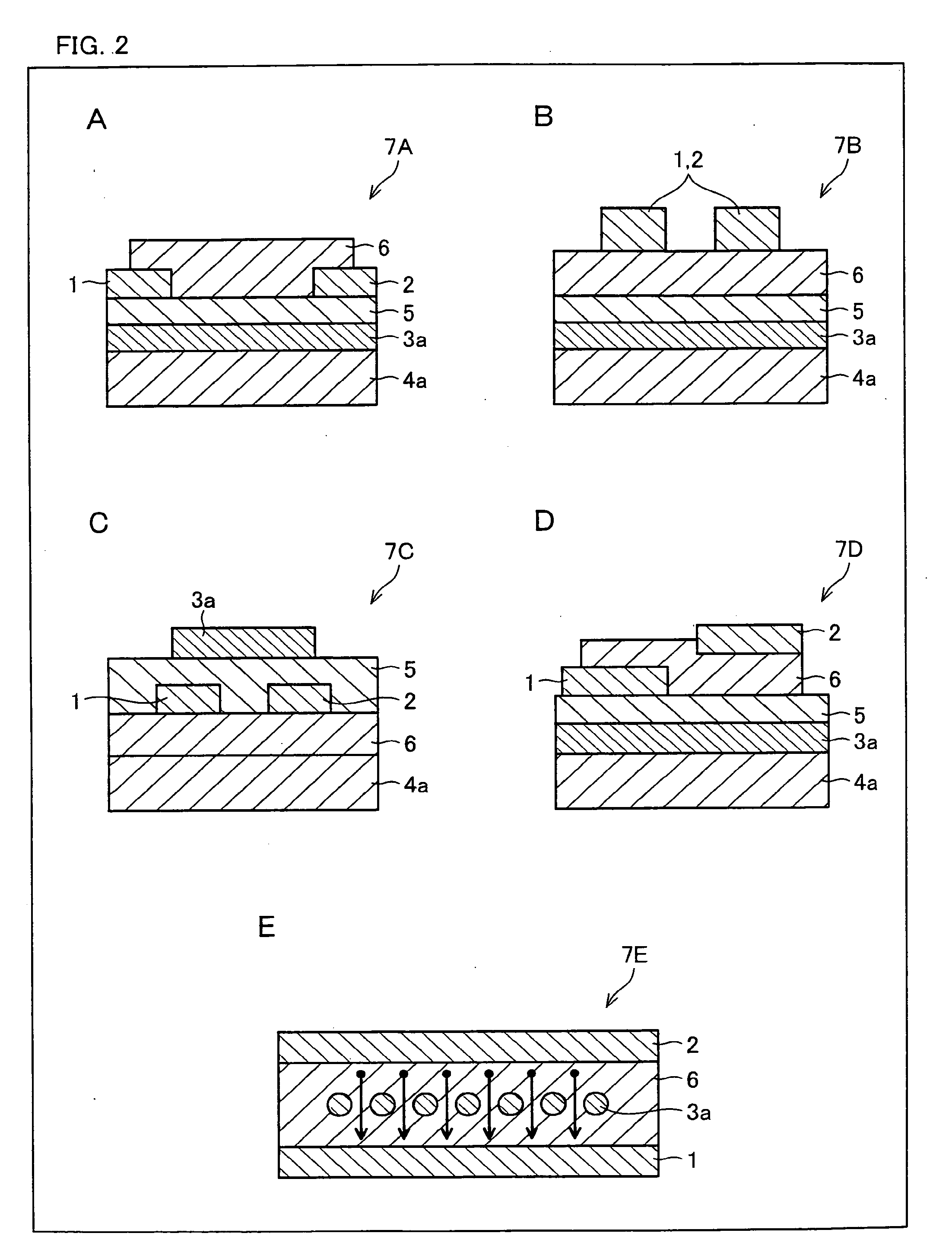
[0170]The following explains still another embodiment of the present invention with reference to FIG. 1. The present embodiment deals with an organic semiconductor device employing the above-described organic semiconductor material as its organic semiconductor material. FIG. 1 is a schematic cross sectional view of a structure of the organic semiconductor device (thin film transistor device), illustrating one embodiment of the present invention.

[0171]The organic semiconductor device in accordance with the present embodiment employs, as the organic semiconductor material, at least one compound selected from the group consisting of (i) the novel fused polycyclic aromatic compounds and (ii) the compounds represented by the general formula (17) obtained by the production method described in Embodiment 2. The organic semiconductor material may include either only one of the compounds or several types of the compounds together, as the fused polycyclic aromatic compound(s). In a case where...


PUM

PropertyMeasurementUnit
Carrier mobilityaaaaaaaaaa
Temperatureaaaaaaaaaa

Abstract

In one embodiment of the present invention, a novel fused polycyclic aromatic compound of the present invention is (a) a compound including a benzodichalcogenophenobenzodichalcogenophene (BXBX) skeleton further having an aromatic ring(s) located outside the BXBX skeleton, or (b) a compound including a BXBX skeleton in which a benzene ring is substituted with a heterocyclic ring. The compound can strengthen intermolecular interaction due to greater π electron orbits. This improves an electron field effect mobility of an organic semiconductor device that is manufactured by use of the compound as an organic semiconductor material. Further, since the number of fused rings included in the compound is small, the compound does not cause problems that generally occur in compounds having an extremely large number of fused rings, i.e., poor solubility in solvent and poor atmospheric stability due to high affinity to oxygen. As a result, the fused polycyclic aromatic compound of the present invention can be preferably used as an organic semiconductor material.

Description

TECHNICAL FIELD[0001]The present invention relates to a novel fused polycyclic aromatic compound, a method for producing the compound, and a use of the compound. More specifically, the present invention relates to (i) a novel fused polycyclic aromatic compound which has electrical, electronic, or photoelectronic properties, and which can be used as a highly soluble organic semiconductor material, (ii) a method for easily producing the compound, and (iii) a use of the compound.BACKGROUND ART[0002]In recent years, thin film devices that employ organic semiconductors such as an organic EL device, an organic FET device, and an organic thin film converting device have been considered noteworthy, and some of the thin film devices have been put into practical use. A fundamental and important property of the organic semiconductors for use in these thin film devices is electron field-effect mobility (carrier mobility).[0003]For example, in organic EL devices, the electron field-effect mobili...

Claims


Application Information

Patent Timeline
IPC IPC(8): H01L51/10H01L51/52C07D495/04
CPCC07C319/14C07C319/20C07C391/02C07D495/04C07D517/04H01L51/0071Y10S428/917H01L51/0558H01L51/0074C07C321/28C07C323/22H10K85/6576H10K85/657H10K10/484H10K50/30
Inventor TAKIMIYA, KAZUOYAMAMOTO, TATSUYA
Owner NIPPON KAYAKU CO LTD
Why Eureka
Try Eureka