

Ultra-Shallow Junctions using Atomic-Layer Doping
a technology of atomic layer and ultrashallow junction, which is applied in the direction of semiconductor devices, transistors, electrical devices, etc., can solve the problems of cmos devices with a short gate length, significant challenges, and the lik
- Summary
- Abstract
- Description
- Claims
- Application Information
AI Technical Summary
Benefits of technology
Problems solved by technology
Method used
Image

Examples
Embodiment Construction
[0016]The making and using of the presently preferred embodiments are discussed in detail below. It should be appreciated, however, that the present invention provides many applicable inventive concepts that can be embodied in a wide variety of specific contexts. The specific embodiments discussed are merely illustrative of specific ways to make and use the invention, and do not limit the scope of the invention.
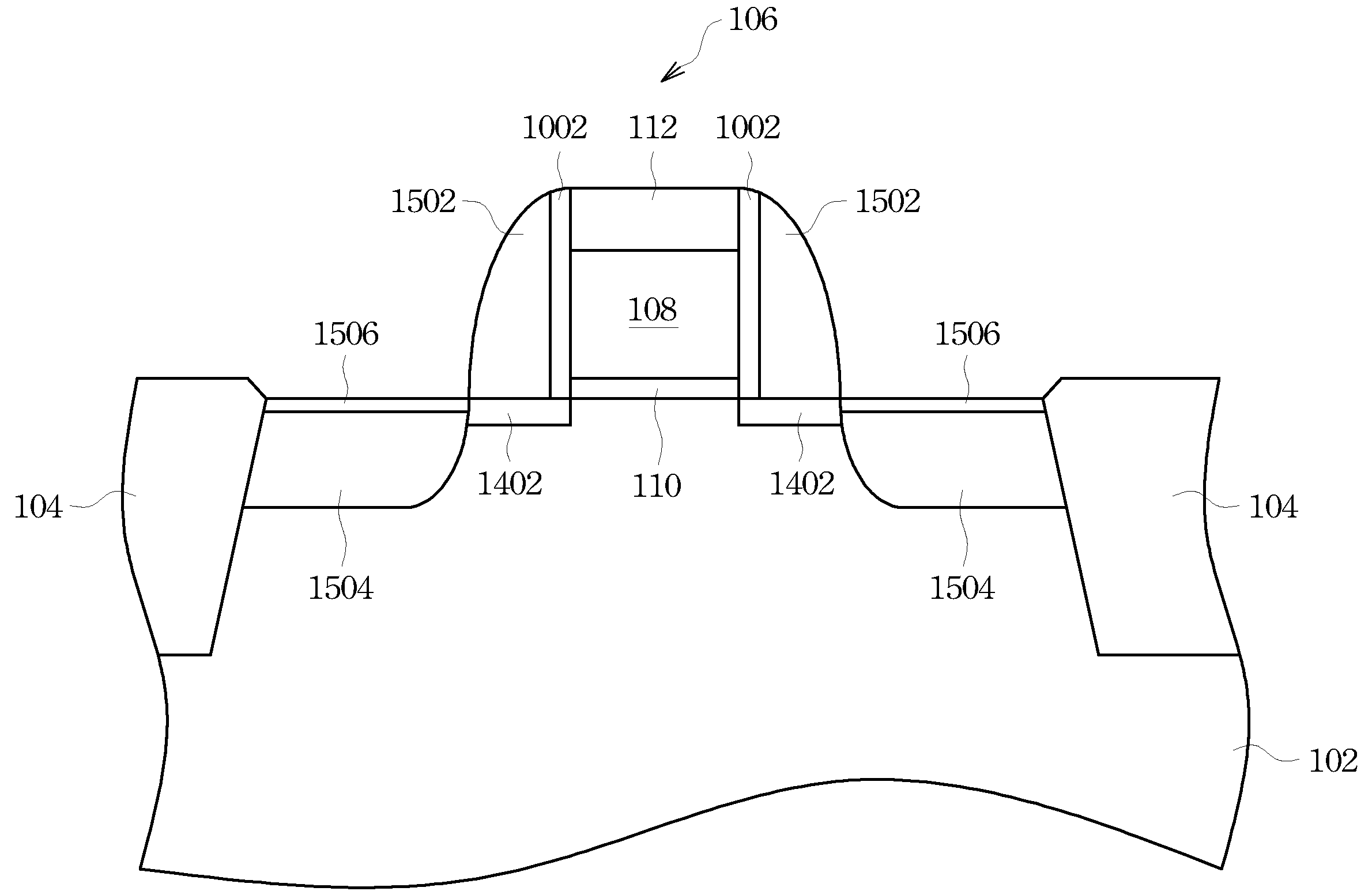
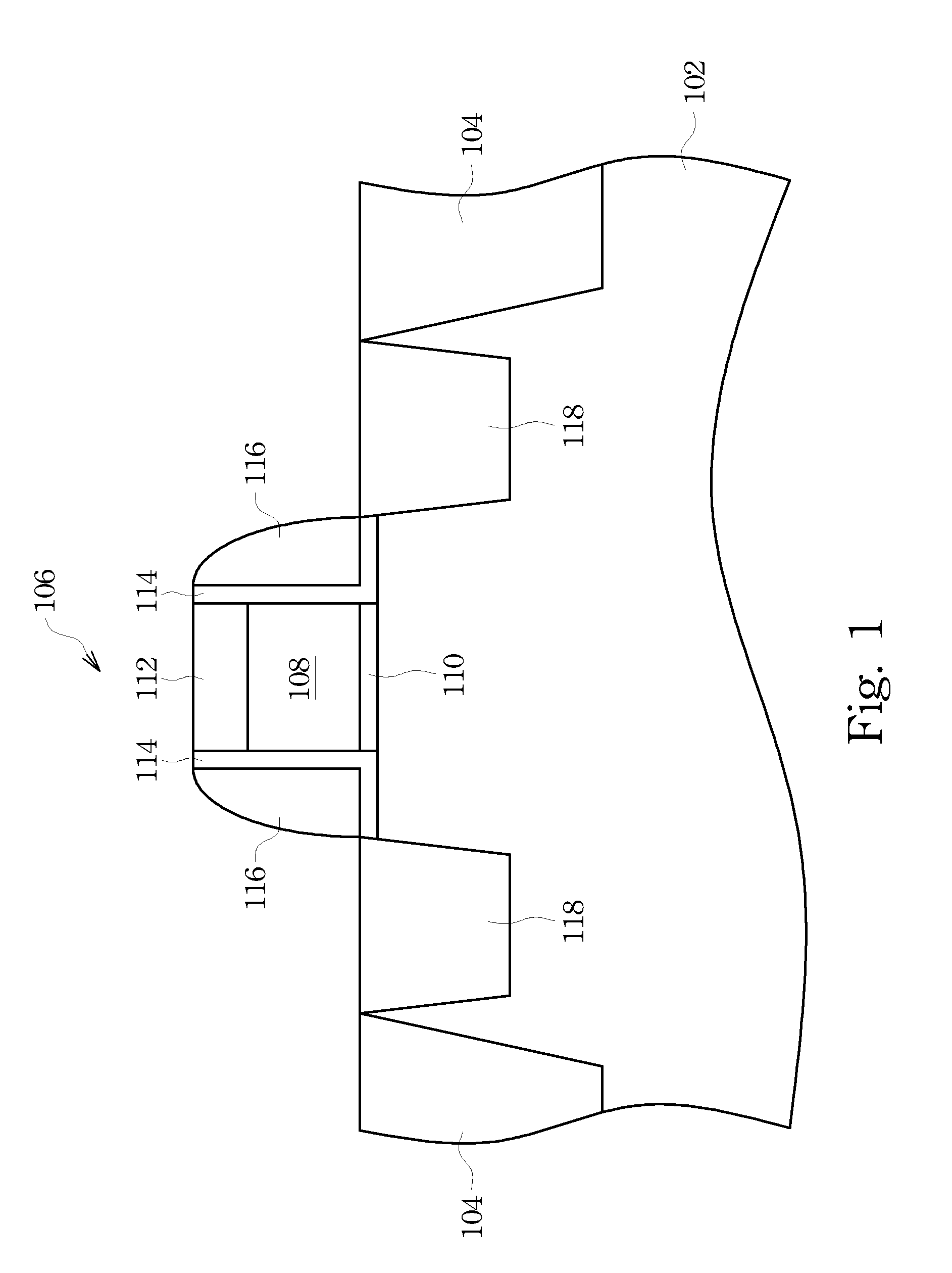
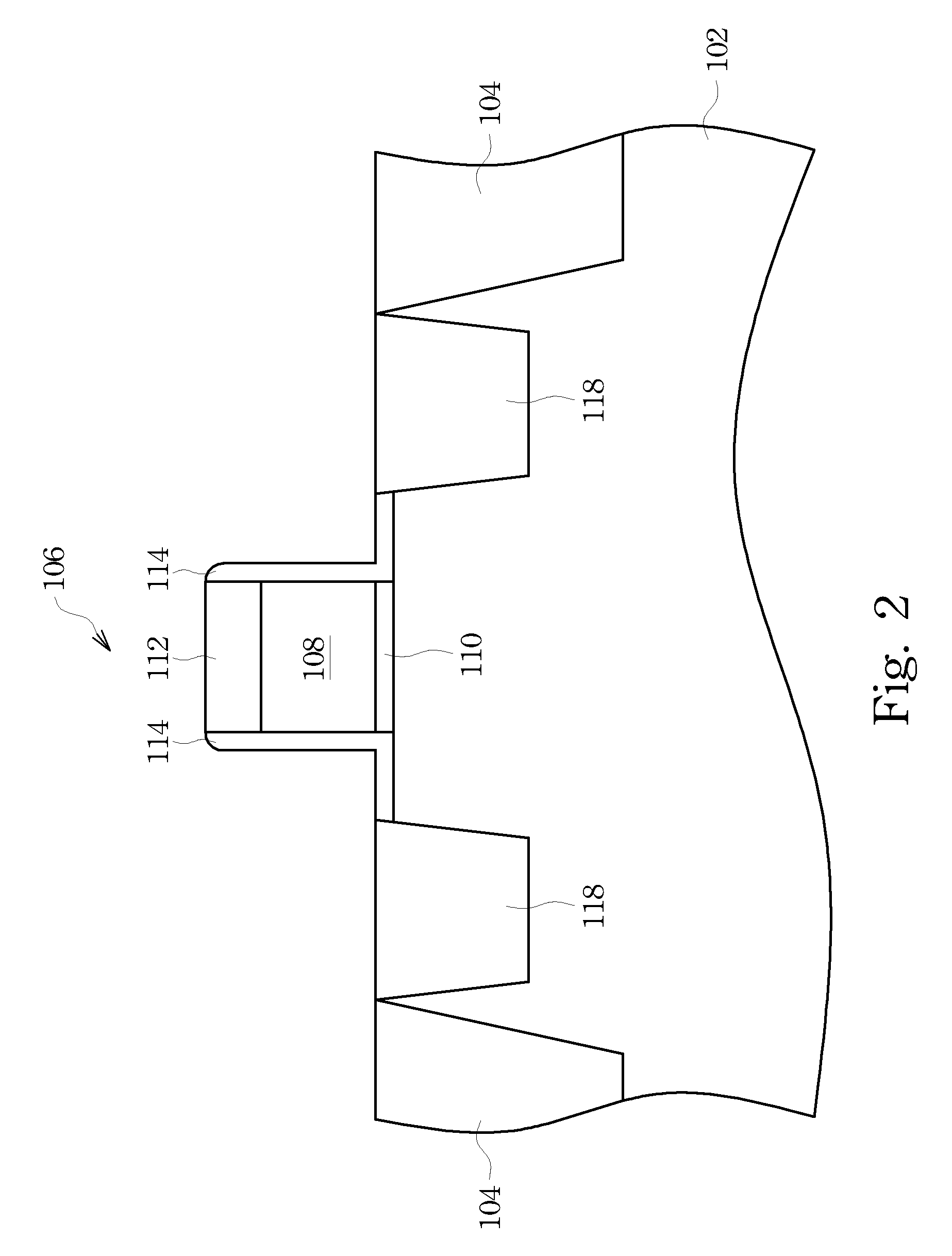
[0017]Referring first to FIGS. 1-7, there is illustrated a first method of forming a transistor having ultra-shallow junctions (USJs) in accordance with an embodiment of the present invention. Referring first to FIG. 1, there is shown a substrate 102 having isolation structures 104 formed therein to define an active region in the substrate 102. The substrate 102 is preferably a silicon substrate, though other materials, such as germanium, quartz, sapphire, and glass, could alternatively be used. Alternatively, the silicon substrate 102 may be an active layer of a semiconducto...
PUM
 Abstract
Description
Claims
Application Information