
Effective efuse structure

Active Publication Date: 2010-03-25
NXP USA INC
View PDF14 Cites 6 Cited by
  • Summary
  • Abstract
  • Description
  • Claims
  • Application Information

AI Technical Summary

Problems solved by technology

This high current is intended to break the eFuse structure which results in an electrical open.
However, if during programming of the eFuse, the silicide in the eFuse is not completely migrated to its anode from its cathode, then the eFuse is rendered non-functional.
In addition, as poly gates are scaled down to smaller and smaller dimensions, the actual poly media portion in an eFuse becomes smaller and smaller, causing silicide migration through the poly medium to become more and more difficult.
Furthermore, it is difficult to produce silicide migration when the medium (e.g., poly) is smaller than a critical dimension.

Method used


Image

  • Effective efuse structure
  • Effective efuse structure
  • Effective efuse structure

Examples


Embodiment Construction

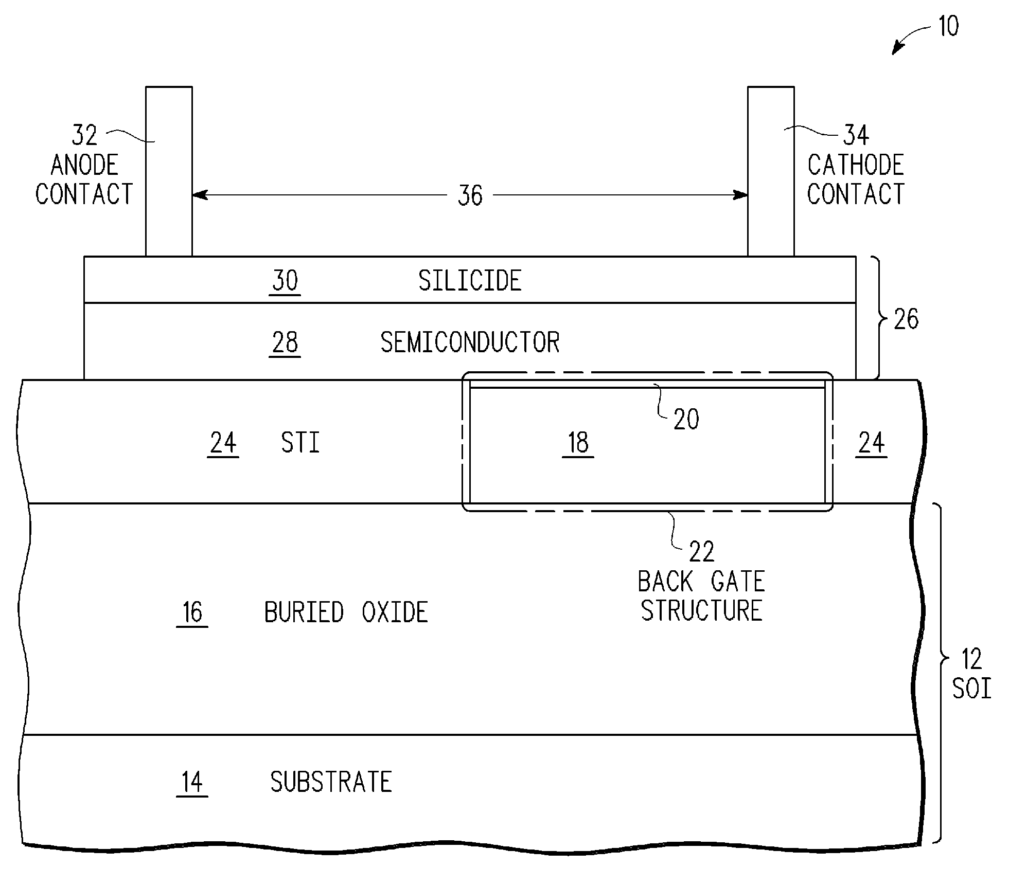
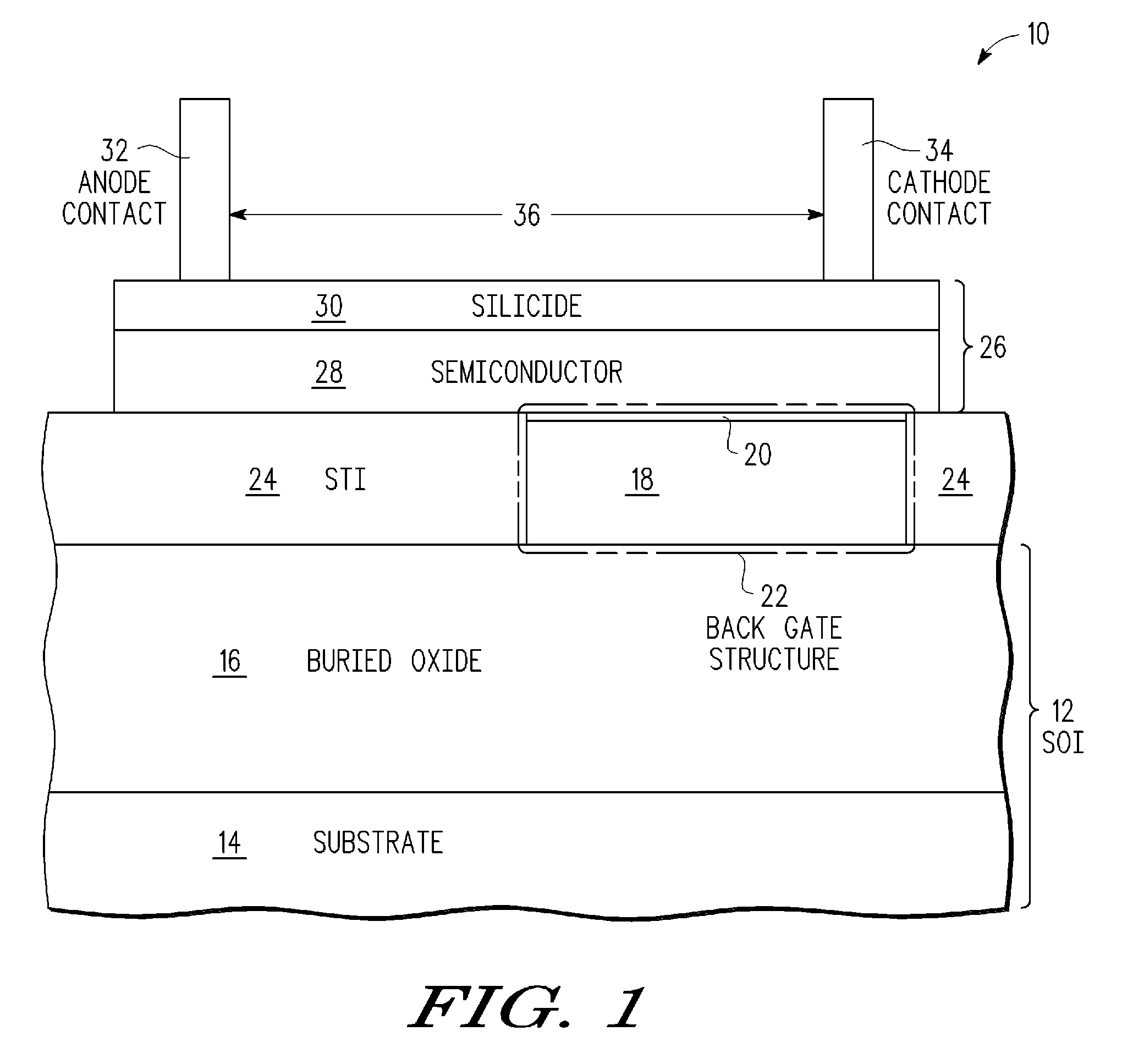
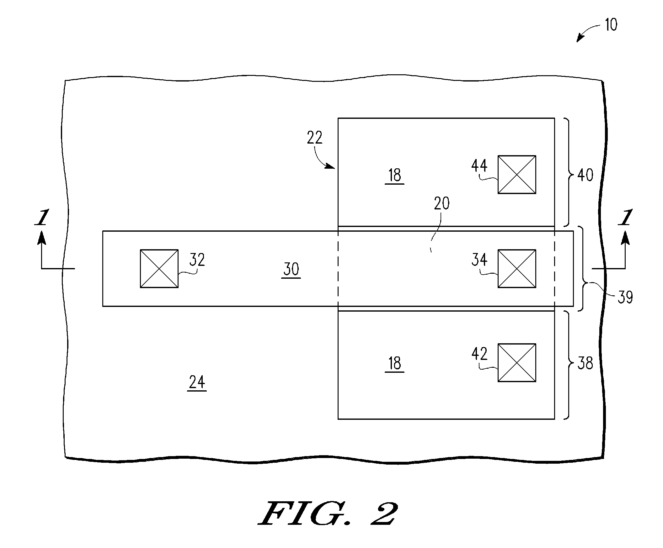
[0014]The embodiments of the present disclosure resolve problems in the art by utilizing a back gate bias under cathode in a novel efuse structure, as discussed herein. With the back gate bias, a silicide migration to anode is enhanced. In one embodiment, a back gate operation can be carried out with use of transistor characteristics. In addition, the introduction of the back gate in an efuse structure advantageously enables an effective eFuse silicide migration.

[0015]The semiconductor substrate described herein can be any semiconductor material or combinations of materials, such as gallium arsenide, silicon germanium, silicon-on-insulator (SOI), silicon, monocrystalline silicon, the like, and combinations of the above.

[0016]FIG. 1 is a cross-sectional view of an electrically programmable fuse structure 10 featuring a back gate structure according to one embodiment of the present disclosure. The electrically programmable fuse 10 includes, for example, an SOI substrate 12 comprising ...


PUM


Abstract

An electrically programmable fuse (eFuse) comprises a semiconductor layer, a silicide layer overlying the semiconductor layer, and first and second contact structures electrically coupled to the silicide layer. The first contact structure is configured to function as an anode and the second contact structure is configured to function as a cathode. The eFuse further comprises a back-gate structure disposed underneath the semiconductor layer in a back-gate structure region proximate the second contact structure, the back-gate structure region excluding a region proximate the first contact structure. Responsive to (i) a programming voltage potential supplied between the first and second contact structures and (ii) a voltage potential supplied to the back-gate structure, silicide of the silicide layer operates to migrate, with an enhanced migration, into the semiconductor layer from the cathode to the anode with an absence of silicide residue in at least the back-gate structure region of the semiconductor layer between the first and second contact structures.

Description

BACKGROUND[0001]1. Field[0002]This disclosure relates generally to an electronically programmable fuse (eFuse), and more specifically, to an improved eFuse structure and method of making the same.[0003]2. Related Art[0004]Electrically programmable fuses (eFuses) generally include a silicide overlying a polysilicon layer, further having a first contact positioned on one end of the silicide and a second contact disposed at a distance from the first contact on an opposite end of the silicide. One contact functions as the anode while the other contact functions as a cathode.[0005]Programming of an eFuse is typically accomplished by forcing a large electrical current through the eFuse. This high current is intended to break the eFuse structure which results in an electrical open. In other words, during programming, it is desirable for the silicide to migrate from the cathode to the anode and thus create an electrical “open” in the silicide.[0006]Furthermore, for conventional eFuse progra...

Claims


Application Information

Patent Timeline
IPC IPC(8): H01L23/525H01L21/44
CPCH01L23/5256H01L2924/0002H01L2924/00
Inventor MIN, BYOUNG W.
Owner NXP USA INC
Learn More