Relief layer and imprint method for making the same

a relief layer and imprinting technology, applied in the field of relief layer and imprinting method, can solve the problem of layer becoming not patternable, and achieve the effects of maintaining shape fidelity, relatively high stability of relief layer comprising such groups, and little shrinkag

Active Publication Date: 2010-03-25
KONINKLIJKE PHILIPS ELECTRONICS NV
View PDF9 Cites 12 Cited by
  • Summary
  • Abstract
  • Description
  • Claims
  • Application Information

AI Technical Summary

Benefits of technology

[0028]In an embodiment of the relief layer the carbon atom is part of any one of a methyl-group, ethyl group or propyl-group. Alkyl groups form the most stable Si—C chemical bonds. Hence stability of the relief layer comprising such groups is relatively high. Thus, a relief layer incorporating methyl groups as the alkyl groups is stable up to 400° C. in ambient atmosphere, therewith extending its field of application towards those requiring resilience against such temperatures. An ethyl-group provides stability up to approximately 300° C. In addition, the mass and volume of these small alkyl groups cause that the organic mass and volume content of a relief layer of siliconoxide having these alkyl-groups is relatively low. This is advantageous in terms of shrinkage of the layers when subjected to heating to remove these organic alkyl-groups.
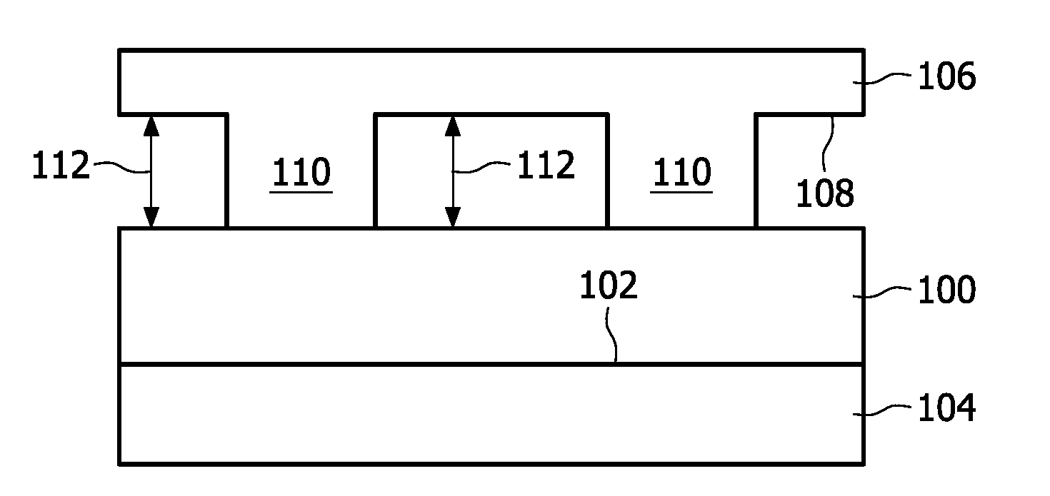
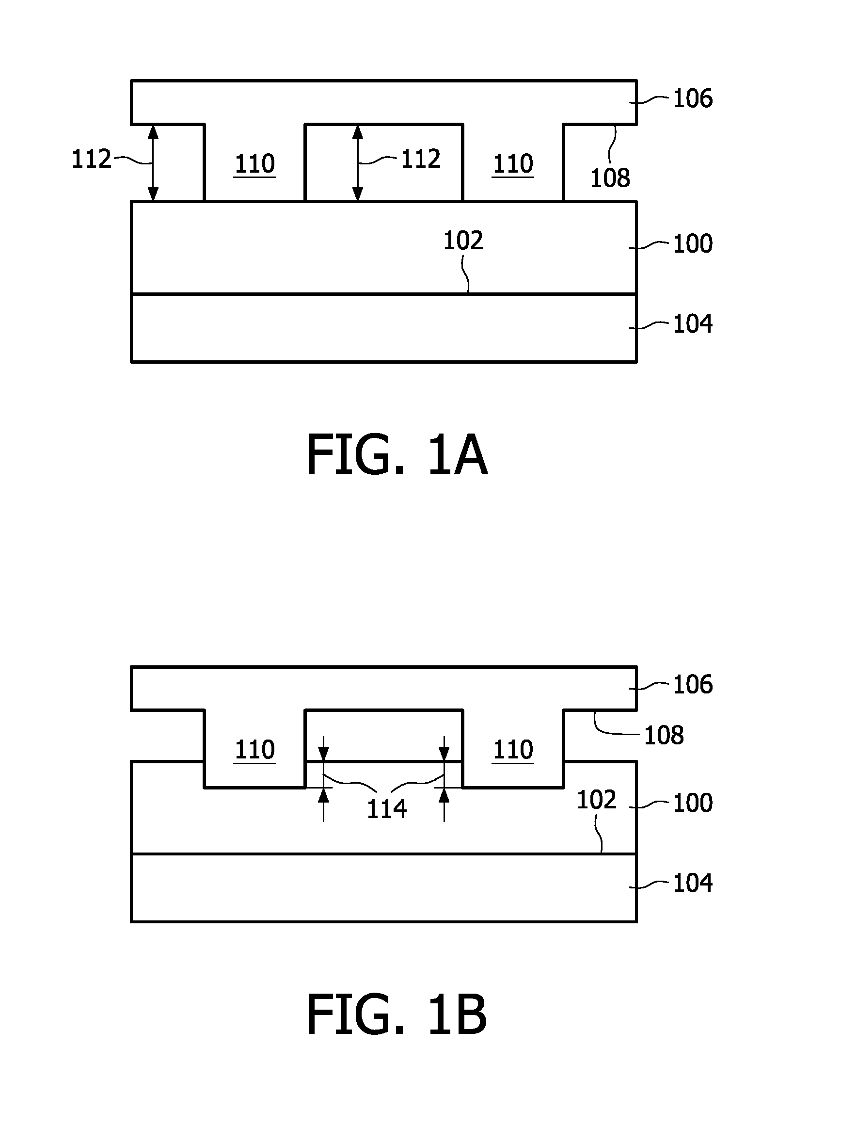
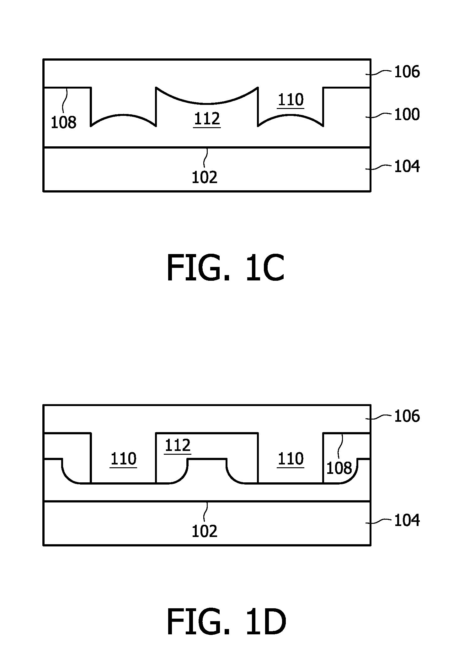
[0029]In an embodiment of the relief layer the features of the relief layer have a shape conformal to the corresponding complementary feature within the template relief surface. Due to the high inorganic mass content within the relief layers, they can be prepared with little shrinkage and shape fidelity is maintained. Especially rounding of corners at the footprint of protrusions of features of the relief layer occurring during solidification of the relief layer is substantially reduced or even absent in a relief layer according to the invention.
[0030]In an embodiment the relief layer is used as an etch mask. The stability of the relief layer and its high inorganic mass content and low porosity make it suitable for use in etching processes requiring harsh conditions such as Reactive ion etching or aggressive wet etching. Hence the layers can be applied as etch masks or hard masks during for example semiconductor manufacturing where such etching is extensively used.
[0031]In an embodiment the relief layer is used for the manufacture of a semiconductor device, optical device or micromechanical device having a functional layer incorporating the relief layer. The stability of the layer based on its structure makes it useful to be implemented as a functional layer within such devices. This is also true for relief layers that can provide specific other functionalities besides the improved strength and integrity.

Problems solved by technology

These requirements however cause the partially dried siliconoxide compound layer to form a highly viscous solution.
Therewith causing the layer to become not patternable especially with flexible or brittle stamps.

Method used


Image

  • Relief layer and imprint method for making the same
  • Relief layer and imprint method for making the same
  • Relief layer and imprint method for making the same

Examples


example 1

[0042]A first siliconoxide compound solution according to the invention is prepared by mixing together 8 gram of Ludox™ TM-50, comprising 50 weight % silica nanoparticles having a particle diameter inbetween 20 nm and −40 nm in water with 1.2 gram of formic acid under stirring. Subsequently, 0.9 gram of Methyltrimethoxysilane (MTMS) is added and the resulting mixture stirred at room temperature for 15 minutes. An additional 6.9 grams of MTMS is added under stirring and the resulting solution is left to stand for 30 minutes at room temperature. Finally 1.7 gram of ethyleneglycolmonobutylether is added. The PH of the resulting silicon compound solution as measured with litmus paper is in between 3.5 and 4.5.

example 2

[0043]A second silicon compound solution according to the invention is prepared by mixing together the silicon compounds precursors MTMS and tetramehoxysilane (TMOS) in a molar ratio as given in table I. In a second step 1M formic acid in water is added to the mixture to an amount of 1 mole water per mole of methoxy-groups of the total added amount of silicon compound precursors. The resulting mixture is allowed to react, undergoing hydrolysis and condensation for period of 10 min. to 30 min. at a temperature between 20° C. and 30° C. in order to form a siliconoxide compound. Then to the mixture is added n-propanol such that the resulting silicon compound solution contains a total Silicon atom concentration of 0.8 mol per kilogram solution. In a final step, water is added to the mixture to an amount of 9 times the total silicon atom content in moles to obtain the silicon compound solution according to the invention.

TABLE ITMOSMTMSWeight % CH3Volume % CH3ExperimentmoleMolein relief l...

example 3

[0045]A third siliconoxide compound solution according to the invention is prepared by mixing together the silicon compounds precursors MTMS and TMOS in a molar ratio as given in table I. Then n-propanol is added to dilute the mixture before in a second step 1M formic acid in water is added to the mixture to an amount of 1 mole water per mole of methoxy-groups of the total added amount of silicon compound precursors. After the addition the resulting mixture is allowed to react, undergoing hydrolysis and condensation for period of 10 min. to 60 min. at a temperature between 20° C. and 30° C. in order to form a siliconoxide compound. In a third step additional n-propanol is added such that the resulting siliconoxide compound solution contains a total silicon atom concentration of 0.8 mol per kilogram solution. In a final step water is added to the mixture to an amount of 9 times the total silicon atom content in moles within the mixture to obtain the siliconoxide compound solution acc...


PUM

PropertyMeasurementUnit
diameteraaaaaaaaaa
temperaturesaaaaaaaaaa
particle diameteraaaaaaaaaa

Abstract

The invention relates to a method for forming a relief layer (216) employing a stamp (206) having a stamping surface (208) including a template relief pattern. A solution comprising a siliconoxide compound (200) is sandwiched between a substrate surface (202) and the stamp surface (208) and dried while sandwiched. After removal of the template relief pattern the relief layer obtained has a high inorganic mass content making it robust and directly usable for a number of applications such as semiconductor, optical or micromechanical.

Description

FIELD OF THE INVENTION[0001]The invention relates to a Method for forming a relief layer employing a stamp having a stamping surface including a template relief pattern. The invention also relates to a relief layer as prepared by the method and the use of such a relief layer in semiconductor, optical and micromechanical devices.BACKGROUND OF THE INVENTION[0002]Providing material layers having a relief pattern can be done using an embossing or imprinting method such as imprinting lithography. In US 2004 / 0264019 A1 an exemplary method is disclosed. In the method, a relatively soft sol-gel layer is provided to a hard surfaced substrate and subjected to an embossing method for forming a pattern in the surface of the layer. To this end a stamp having a stamping surface including the complementary pattern of the desired pattern is used to emboss, i.e. to mold the desired pattern in the upper surface of the relatively soft sol-gel layer.[0003]It is further disclosed that a suitable sol-gel...

Claims


Application Information

Patent Timeline
Patent Type & Authority Applications(United States)
IPC IPC(8): B32B27/28B29C59/02
CPCB82Y10/00Y10T428/24479G03F7/0002B82Y40/00B29C2059/023
Inventor VERSCHUUREN, MARCUS ANTONIUS
Owner KONINKLIJKE PHILIPS ELECTRONICS NV
Why Eureka
Try Eureka