Trench metal oxide-semiconductor transistor and fabrication method thereof

a metal oxide semiconductor and fabrication method technology, applied in the direction of semiconductor devices, basic electric elements, electrical appliances, etc., can solve the problems of unpreventable, difficult to control the profile of the implant, and the impurity distribution is bad for implant profile control, so as to improve the profile of the well

Inactive Publication Date: 2010-04-01
NIKO SEMICON
View PDF6 Cites 31 Cited by
  • Summary
  • Abstract
  • Description
  • Claims
  • Application Information

AI Technical Summary

Benefits of technology

[0014]It is a main object of the present invention to improve the profile of the well of the trench metal oxide semiconductor transistor so as to prevent the bottom of the gate trench from being covered by the well to result in failure.

Problems solved by technology

In order to catch up the requirements of power saving and low energy loss, converters with higher power conversion efficiency, which brings the circuit designers a more severe challenge, are unpreventable.
Such impurity distribution is bad for implant profile control.

Method used


Image

  • Trench metal oxide-semiconductor transistor and fabrication method thereof
  • Trench metal oxide-semiconductor transistor and fabrication method thereof
  • Trench metal oxide-semiconductor transistor and fabrication method thereof

Examples


Embodiment Construction

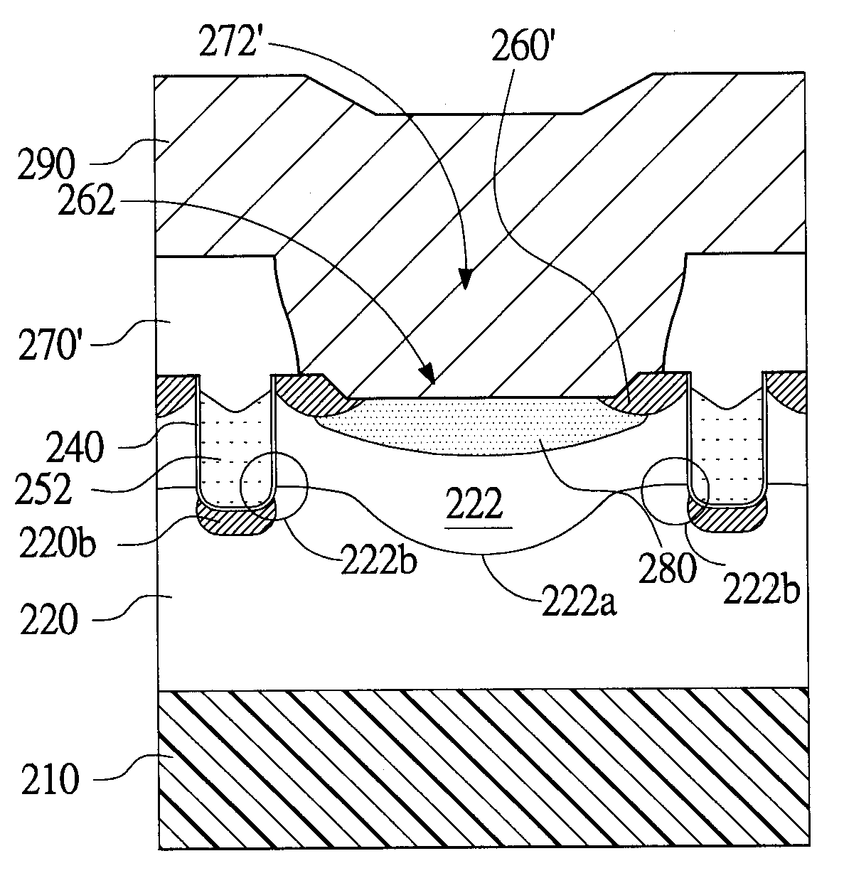
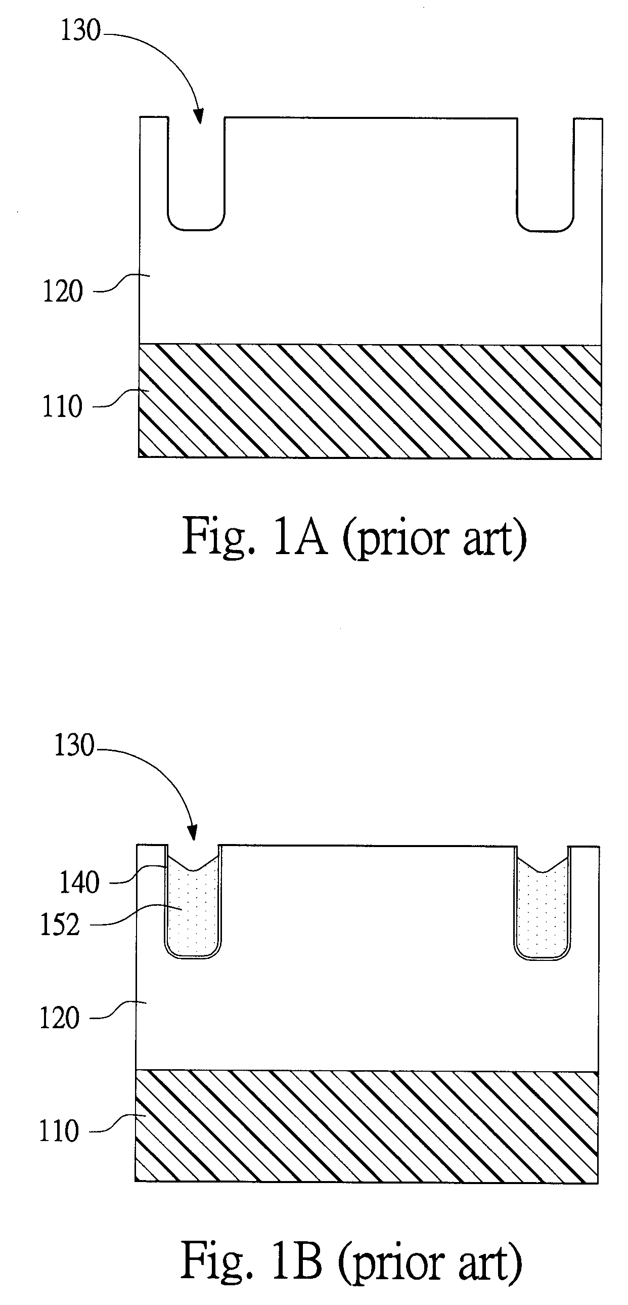
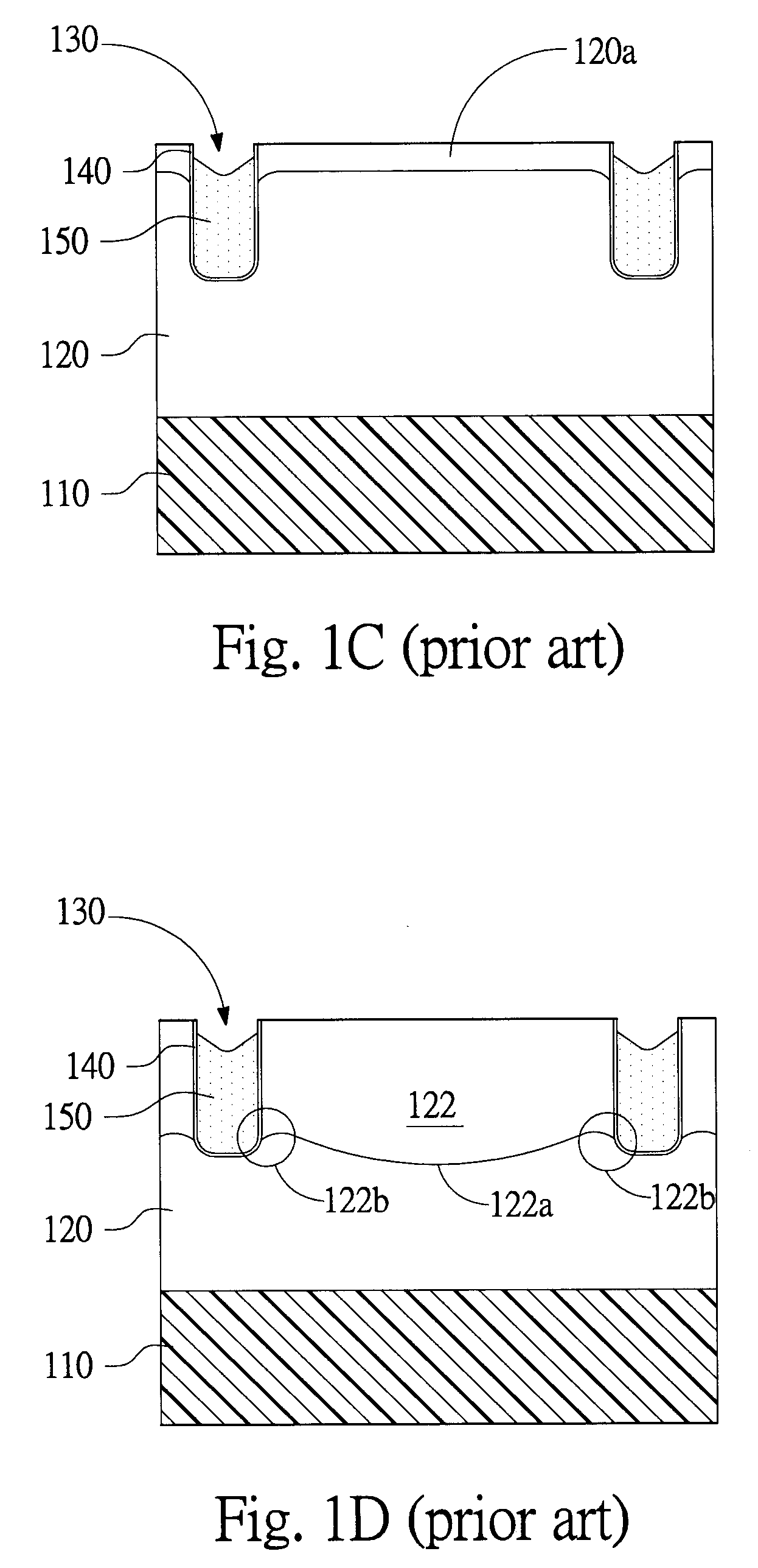
[0023]FIGS. 2A to 2H are schematic views showing a preferred embodiment of a fabrication method of the trench metal oxide semiconductor transistor in accordance with the present invention. N-type metal oxide semiconductor transistor is taken for example. Referring to FIG. 2A, firstly, an N-type epitaxial layer 220 is formed over an N-type silicon substrate 210. Afterward, the location of gate is defined on the epitaxial layer 220 by using a mask (not shown) and a dry etch process is carried out to form a plurality of gate trenches 230 in the epitaxial layer 220. Thereafter, N-type impurities are implanted to the surface region 220a of the epitaxial layer 220 and the bottom region 220b of the gate trench 230 by using the blanket implant technology.

[0024]Thereafter, referring to FIG. 2B, a gate oxide layer 240 is formed on the inner walls of the gate trenches 230. Then, a polysilicon pattern 250 is formed on the epitaxial layer 220 to fill the gate trenches 230 and covers a predetermi...


PUM


Abstract

A fabrication method of a trench metal oxide-semiconductor (MOS) transistor is provided. After the gate trenches are formed in the epitaxial layer, impurities of a first conductive type are implanted into the epitaxial layer by using a blanket implantation process. A polysilicon pattern filling the gate trenches and covering a predetermined range of epitaxial layer surrounding the gate trenches is formed on the epitaxial layer. Impurities of a second conductive type are implanted through the polysilicon pattern into the epitaxial layer to form a well. Impurities of the first conductive type are implanted to form a plurality of first doping regions. A portion of the polysilicon layer above the upper surface of the epitaxial layer is removed by etching to form a plurality of polysilicon gates. Impurities in the first doping regions are driven in to form a plurality of source regions adjacent to the gate trenches.

Description

BACKGROUND OF THE INVENTION[0001]1. Field of the Invention[0002]This invention relates to a metal oxide semiconductor transistor and a fabrication method thereof, and more particularly relates to a trench metal oxide semiconductor transistor and a fabrication method thereof.[0003]2. Description of Related Art[0004]In order to catch up the requirements of power saving and low energy loss, converters with higher power conversion efficiency, which brings the circuit designers a more severe challenge, are unpreventable. To overcome this challenge, the newly developed power elements play an important role. In present, the power metal oxide semiconductor field effect transistor (MOSFET) has been widely adopted to various power converters.[0005]Energy loss of the power metal oxide semiconductor field effect transistor (MOSFET) includes conduction loss resulted from on-resistance and energy loss resulted from inter-electrode capacitance (including output capacitance Ciss and reverse transfe...

Claims


Application Information

Patent Timeline
Patent Type & Authority Applications(United States)
IPC IPC(8): H01L29/78H01L21/336
CPCH01L29/0878H01L29/1095H01L29/7813H01L29/66727H01L29/66734H01L29/41766
Inventor TU, KAO-WAYTUNG, CHENG-HUITSAI, HSIAO-WEI
Owner NIKO SEMICON
Why Eureka
Try Eureka