Mounting structure of electronic component and method of manufacturing electronic component

a technology of electronic components and mounting structures, which is applied in the direction of electrical apparatus casings/cabinets/drawers, oscillator generators, coatings, etc., can solve the problems of degrading reliability and connection reliability, and achieve the effect of preventing degradation of electronic component characteristics, and preventing the influence of outgas generated from resin

Inactive Publication Date: 2010-04-01
SEIKO EPSON CORP
View PDF0 Cites 8 Cited by
  • Summary
  • Abstract
  • Description
  • Claims
  • Application Information

AI Technical Summary

Benefits of technology

[0006]An advantage of the invention is to provide a mounting structure of an electronic component and a method of manufacturing an electronic component capable of preventing degradation of electronic component characteristic by preventing influence of the outgas.
[0007]According to a first aspect of the invention, a mounting structure includes: an electronic component including: a functional element having a predetermined function; a first resin protrusion section having a surface covered by a covering film including a conductive section electrically connected to the functional element; and a second resin protrusion section that is disposed inside an area surrounded by the first resin protrusion section, and has adhesiveness at least on a surface of the second resin protrusion section, and a base member having a connection electrode and adapted to mount the electronic component. In the structure, the second resin protrusion section mounts the electronic component on the base member in a condition in which the conductive section of the covering film has conductive contact with the connection electrode due to elastic deformation of the first resin protrusion section.
[0008]According to the mounting structure of an electronic component of the first aspect of the invention, there can be obtained a structure in which the first resin protrusion section covered by the covering film is used as the electrical contact and the second resin protrusion section is made to function as the bonding material, thereby mounting the electronic component on the base member while keeping the preferable conducting state. Here, since the first resin protrusion section is covered by the covering film, the influence of the outgas generated from the resin can be prevented. Further, since the second resin protrusion section is surrounded by the first resin protrusion section in the periphery thereof, thereby being put into the sealed condition. Thus, the influence of the outgas generated from the second resin protrusion section can be prevented. Therefore, degradation of the characteristic of the electronic component due to the outgas can be prevented. Further, since both of the first and second resin protrusion sections have elasticity, the load to the conducting section can be reduced even in the case in which an external impact is applied, thus superior conducting reliability can be obtained.
[0009]Further, in the mounting structure of an electronic component of the first aspect of the invention, it is preferable that the functional element be a quartz crystal element.
[0010]In the first aspect of the invention, the electronic component configures the quartz crystal resonator provided with the quartz crystal element. Therefore, the deterioration of the vibration characteristic of the quartz crystal resonator due to the outgas can be prevented as described above, and the quartz crystal resonator provided with high conducting reliability can be obtained.
[0011]Further, in the mounting structure of an electronic component of the above aspect of the invention, it is preferable that the first resin protrusion section and the second resin protrusion section be made of a same photosensitive resin material.

Problems solved by technology

In the case of using such a conductive paste, the connecting section between the quartz crystal resonator and each of the connection electrodes might be damaged when an impact such as a drop impact is applied thereto, which is a factor for degrading connection reliability.
However, in the case of adopting such a bump electrode, outgas generated from the adhesive might change the vibration characteristic of the quartz crystal resonator, thereby degrading the reliability.

Method used


Image

  • Mounting structure of electronic component and method of manufacturing electronic component
  • Mounting structure of electronic component and method of manufacturing electronic component
  • Mounting structure of electronic component and method of manufacturing electronic component

Examples


Embodiment Construction

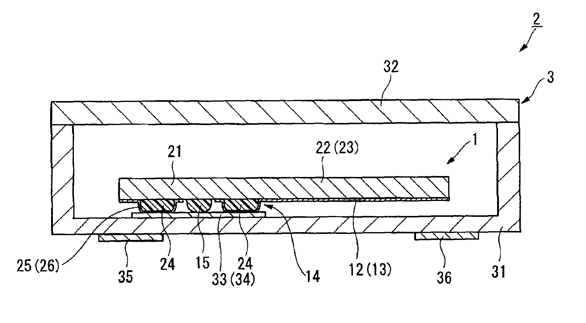
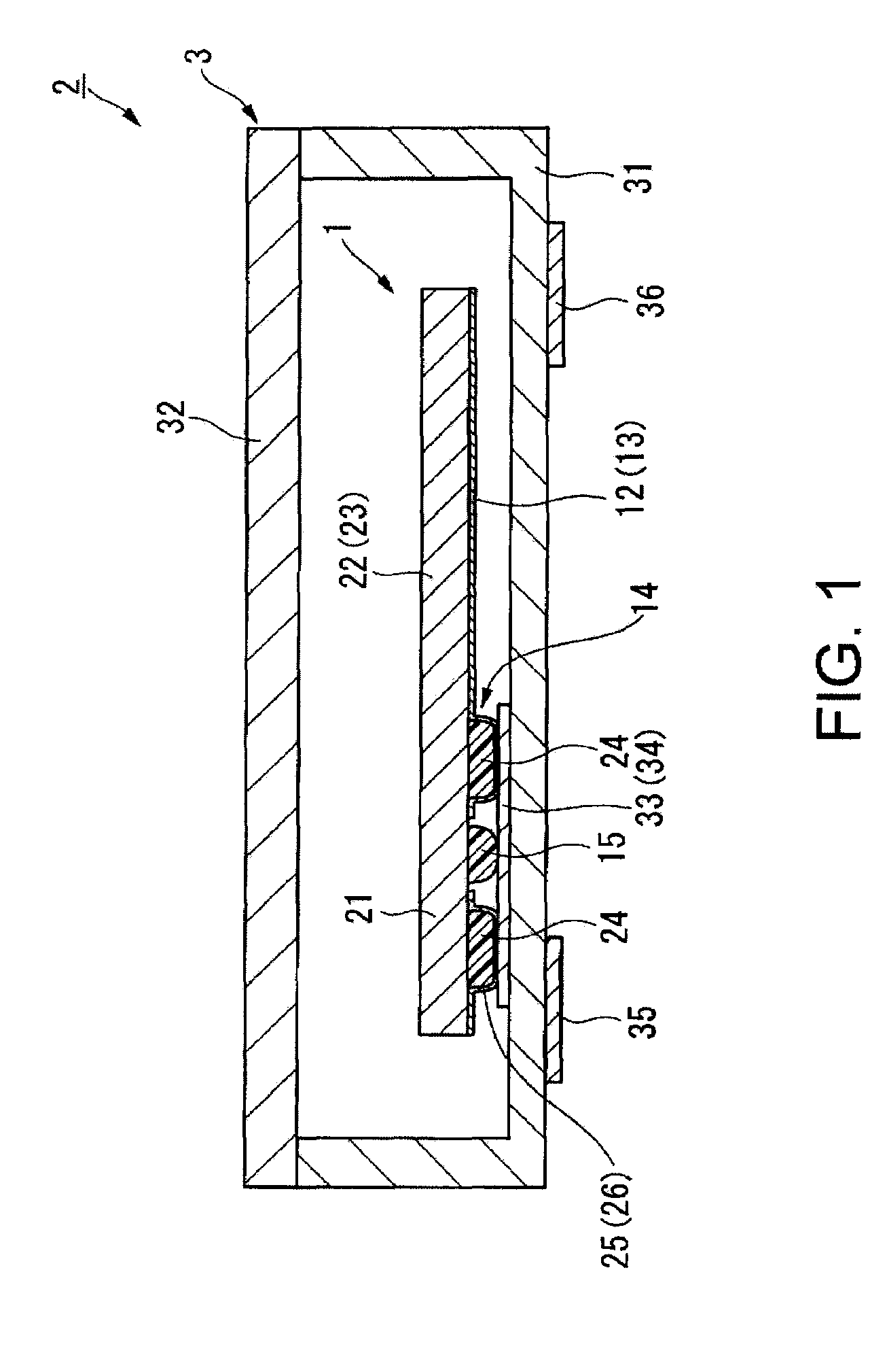
[0030]An embodiment of the invention will hereinafter be explained with reference to the drawings. It should be noted that the scale size of each member is accordingly altered so that the member is shown large enough to be recognized in the drawings used in the following explanations.

[0031]FIG. 1 is a diagram showing a quartz crystal resonator package adopting a mounting structure of an electronic component according to the present embodiment of the invention. FIG. 1 is a diagram showing a cross-sectional configuration of the quartz crystal resonator package, FIG. 2 is a plan view corresponding to FIG. 1, and FIG. 3 is a bottom view of the quartz crystal resonator. Further, FIGS. 4A and 4B are cross-sectional configuration diagrams corresponding to the view along the A-A′ line shown in FIG. 3, and are diagrams for explaining a shape of a resin protrusion.

[0032]The quartz crystal resonator package (the mounting structure of an electronic component) 2 is provided with a quartz crystal...


PUM


Abstract

A mounting structure includes: an electronic component including: a functional element having a predetermined function; a first resin protrusion section having a surface covered by a covering film including a conductive section electrically connected to the functional element; and a second resin protrusion section that is disposed inside an area surrounded by the first resin protrusion section, and has adhesiveness at least on a surface of the second resin protrusion section, and a base member having a connection electrode and adapted to mount the electronic component. In the structure, the second resin protrusion section mounts the electronic component on the base member in a condition in which the conductive section of the covering film has conductive contact with the connection electrode due to elastic deformation of the first resin protrusion section.

Description

BACKGROUND[0001]1. Technical Field[0002]The present invention relates to a mounting structure of an electronic component, and a method of manufacturing an electronic component.[0003]2. Related Art[0004]An electronic component such as a quartz crystal resonator including a functional element is fixed in the state in which excitation electrodes provided to the quartz crystal resonator and connection electrodes for connecting the quartz crystal resonator to a drive circuit have conductive contact with each other via a conductive paste such as a solder paste (see, e.g., JP-A-11-261360). In the case of using such a conductive paste, the connecting section between the quartz crystal resonator and each of the connection electrodes might be damaged when an impact such as a drop impact is applied thereto, which is a factor for degrading connection reliability.[0005]Therefore, it is possible to adopt a mounting structure of an electronic component in which a bump electrode composed of a core ...

Claims


Application Information

Patent Timeline
Patent Type & Authority Applications(United States)
IPC IPC(8): H05K5/00B05D5/12H03B1/00
CPCH03H9/1021H03H9/0519
Inventor HASHI, YUKIHIRO
Owner SEIKO EPSON CORP
Why Eureka
Try Eureka