Novel capacitors and capacitor-like devices

a technology of capacitors and capacitors, applied in the direction of fixed capacitors, fixed capacitor details, thin/thick film capacitors, etc., can solve the problems of high cost of changes, limited transmission speed of such transmission lines, and all electronic devices that use or are affected, so as to enhance or reduce the capacity of devices

Inactive Publication Date: 2010-04-08
KOPP THILO +1
View PDF4 Cites 27 Cited by
  • Summary
  • Abstract
  • Description
  • Claims
  • Application Information

AI Technical Summary

Benefits of technology

[0028]By inserting MAIs into practical devices, the capacities of the devices are enhanced or decreased as compared to the value given by Eq. 1 and novel architectures f

Problems solved by technology

Today, practically all electronic devices use or are affected—often undesired—by the induction of charges due to electric fields.
The transmission speed of such transmission lines is limited by the time needed to charge the capacitor formed by the transmission line, the surrounding dielectric material, and other conducting circuit components that act as counter-electrodes;Piezoelectric and ferroelectric devices.
Yet, such changes are costly, and future changes to even higher κ materials will be even more so.

Method used


Image

  • Novel capacitors and capacitor-like devices
  • Novel capacitors and capacitor-like devices
  • Novel capacitors and capacitor-like devices

Examples


Embodiment Construction

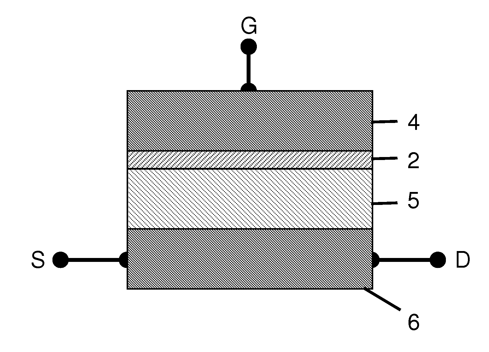
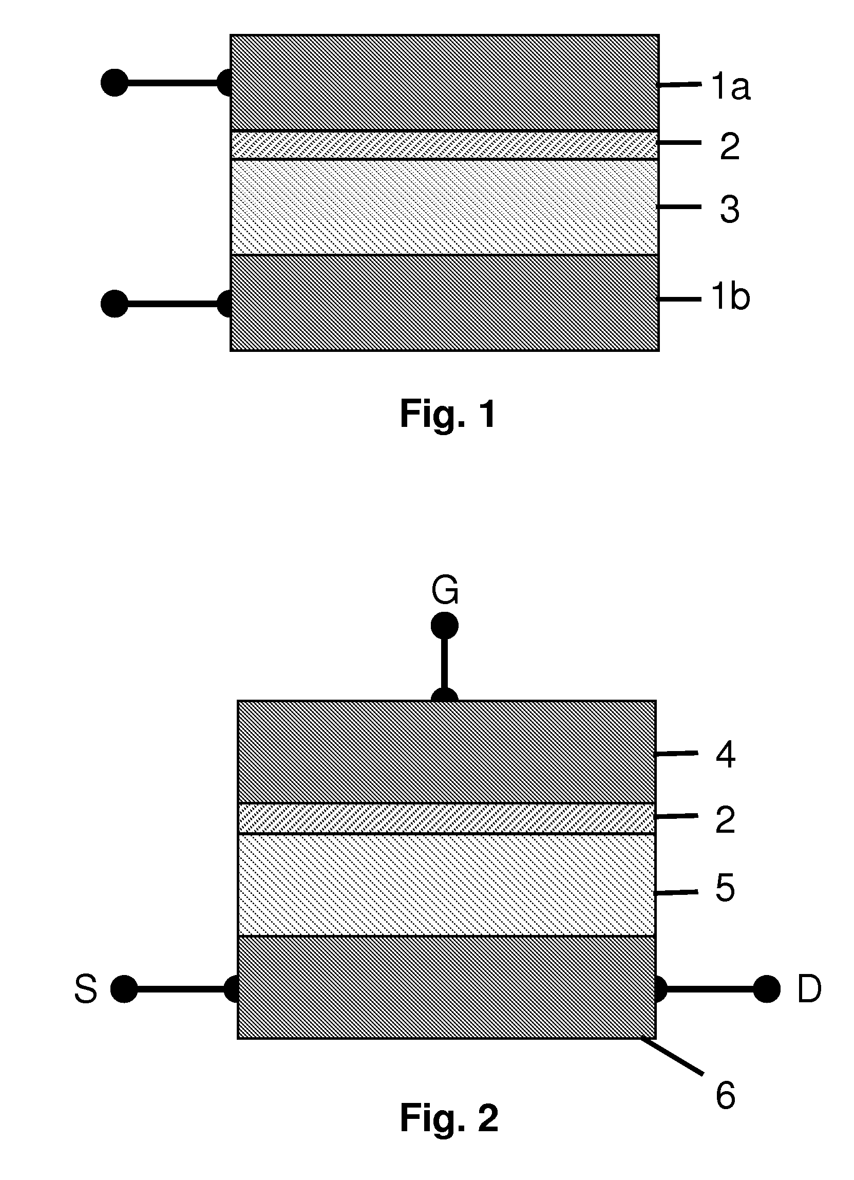
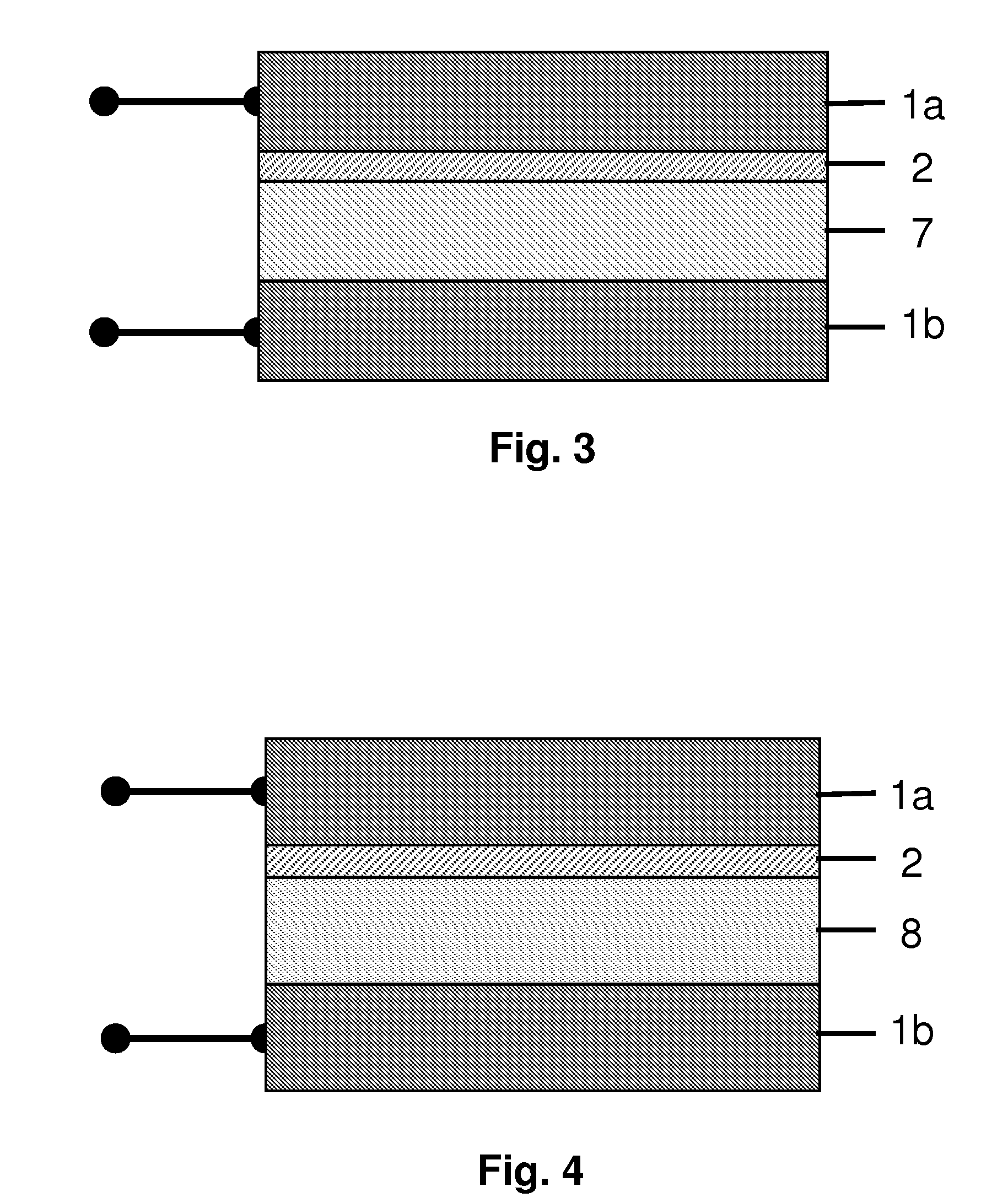
[0041]FIG. 1 illustrates a capacitor according to the invention with electrodes 1a and 1b separated by a standard dielectric 3. The capacity of this capacitor is altered by an MAI layer 2.

[0042]A capacitor according to the invention is shown in FIG. 1. Therein, the electrostatic property—and thus the capacitance—is determined by the MAI 2 and the dielectric 3. In such a configuration, even a 2D-electron gas of a semiconducting heterostructure may be integrated into a practical capacitor.

[0043]Preferable dimensions are:[0044]a dielectric 3 having a thickness of less than (20 nm×εr), εr being the dielectric constant of the dielectric material used; and[0045]an MAI of less than 50 nm thickness.

[0046]Thus, if air is the dielectric, the resulting thickness of the dielectric should be less than 20 nm. If a dielectric material with a high dielectric constant, e.g. larger than 10, is used, the dielectric may have a preferable thickness of less than 200 nm. Altogether, the thickness of the d...


PUM


Abstract

A capacitor and capacitor-like device or any other device showing capacitive effects, including FETs, transmission lines, piezoelectric and ferroelectric devices, etc., with at least two electrodes, of which at least one electrode consists of or comprises a material or is generated as electron system, whose absolute value of the electronic charging energy as defined by the charging-induced change of Ekin+Eexc+Ecorr exceeds 10% of the charging-induced change of the Coulomb field energy of the capacitor according to E=Ecoul+Ekin+Eexc+Ecorr. Therein, E is the energy of a capacitor and Ecoul=Q2/2 Ccoul=Q2d/(2ε0 εx A), A is the area of the capacitor electrodes, d is the distance and ε0εx the dielectric constant between them. Ecorr describes the correlation energy, Ekin the electronic kinetic energy and Eexc the exchange energy of the electrode material. Particularly in miniaturized devices, Ecoul is becoming so small that, by using certain materials or material combinations for the capacitor, Ekin, Eexc, and/or Ecorr provide significant contributions to E. Preferred are materials with strongly correlated electron systems such as perovskites like La1-xSrxTiO3, YBa2Cu3O7-d, vanadates such as (V1-xAx)2O3 with A=Cr, Ti, materials with free electron gases of typically low densities such as Cs, Bi or Rb, or of materials the carrier density of which is reduced by diluting these materials in other materials with smaller carrier densities, metals like Fe, or Ni, materials with van-Hove singularities in the electronic density of states such as graphite or Bechgaard salts or even or 2D-electron gases generated by graphene or by heterostructures, such as the electron gases generated at LaAlO3/SrTiO3 or ZnO/(MgxZn1-x)O multilayers and more.

Description

CROSS-REFERENCE TO RELATED APPLICATION[0001]This application claims priority under 35 U.S.C. §119 to U.S. Provisional Application Nos. 61 / 102,174, filed Oct. 2, 2008 and 61 / 152,389 filed on Feb. 13, 2009, the entire disclosure of which is incorporated herein by reference.TECHNICAL FIELD AND BACKGROUND OF THE INVENTION[0002]The present invention relates to capacitors and capacitor-like devices, in principle to any device showing capacitive effects, particularly in miniaturized devices like integrated circuits. Today, practically all electronic devices use or are affected—often undesired—by the induction of charges due to electric fields. Examples are[0003]Field effect transistors, such as MOSFETs, in which charging of the gate capacitors is used to turn the conductivity of drain-source channels on and off;[0004]Transmission lines used to transmit voltage pulses in integrated circuits. The transmission speed of such transmission lines is limited by the time needed to charge the capaci...

Claims


Application Information

Patent Timeline
IPC IPC(8): H01L29/92H01G4/00H01G4/008
CPCH01G4/008H01G4/33H01L28/57H01L41/0478H01L29/1606H01L29/94H01L41/0477H01L28/60H10N30/878H10N30/877
Inventor KOPP, THILOMANNHART, JOCHEN DIETER
Owner KOPP THILO
Why Eureka
Try Eureka