

Method of driving a semiconductor memory device and a semiconductor memory device
a technology of memory device and semiconductor, applied in the direction of solid-state devices, digital storage, instruments, etc., can solve the problems of increasing the influence of bit line disturbance, deterioration of opposite data stored in unselected memory cells that share a bit line with the selected memory cell, and failure to retain data
- Summary
- Abstract
- Description
- Claims
- Application Information
AI Technical Summary
Benefits of technology
Problems solved by technology
Method used
Image

Examples
first embodiment
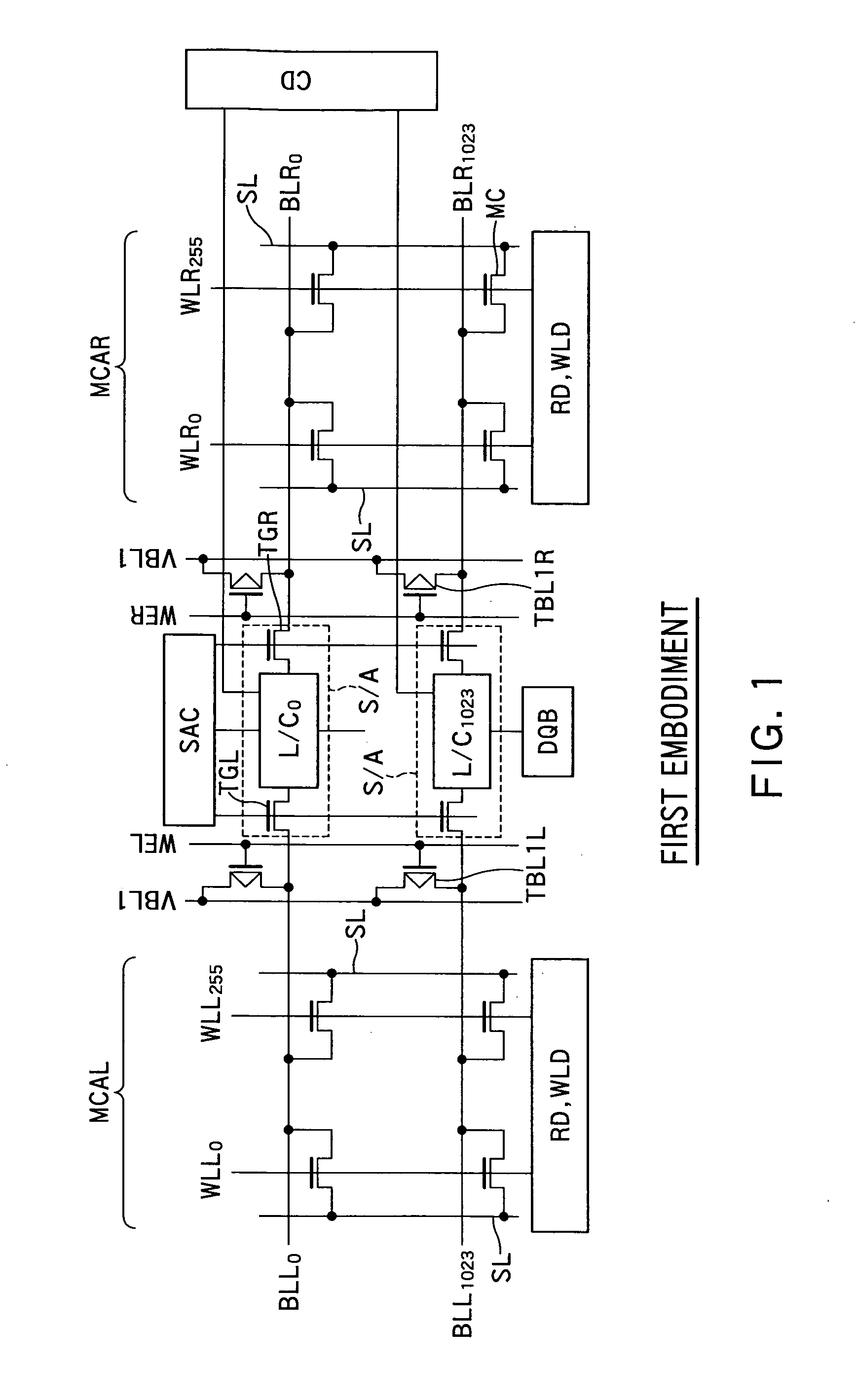
[0071]FIG. 1 is a schematic diagram showing an example of a configuration of an FBC memory device according to a first embodiment of the present invention. An FBC memory device 100 includes memory cells MCs, word lines WLL0 to WLL255 and WLR0 to WLR255 (hereinafter, also “WLs”, “WLL” or “WLR”), bit lines BLL0 to BLL1023 and BLR0 to BLR1023 (hereinafter, also “BLs”, “BLL” or “BLR”), sense amplifiers S / As, source lines SLs, a row decoder RD, a word line driver WLD, a column decoder CD, a sense amplifier controller SAC, and a DQ buffer DQB.
[0072]The memory cells MCs are two-dimensionally arranged in a matrix and constitute memory cell arrays MCAL and MCAR (hereinafter, also “MCAs”). Each of the word lines WLs extends in a row direction and is connected to a gate of each of the memory cells MCs. 256 word lines WLs are arranged on each of the left and the right of the sense amplifiers S / As. Each of the bit lines BLs extends in a column direction and is connected to a drain of each of the...
second embodiment
[0111]FIG. 8 is an explanatory diagram showing a method of driving an FBC memory device according to a second embodiment of the present invention. The second embodiment differs from the first embodiment in the second cycle. Since the first cycle according to the first embodiment is the same as that according to the first embodiment, it will not be described herein.
[0112]In the second cycle according to the second embodiment, holes are extracted from the selected memory cell MC00 out of the memory cells MC00 and MC10 connected to the selected word line WL0. Data “0” is thereby written to the selected memory cell MC00. Holes in small quantity are extracted from the unselected memory cell MC10 out of the memory cells MC00 and MC10 connected to the selected word line WL0. Data “1” is thereby written to the unselected memory cell MC10.
[0113]In the second cycle, the potential of the selected word line WL0 is a potential biased to the same polarity as that of majority carriers in the memor...
third embodiment
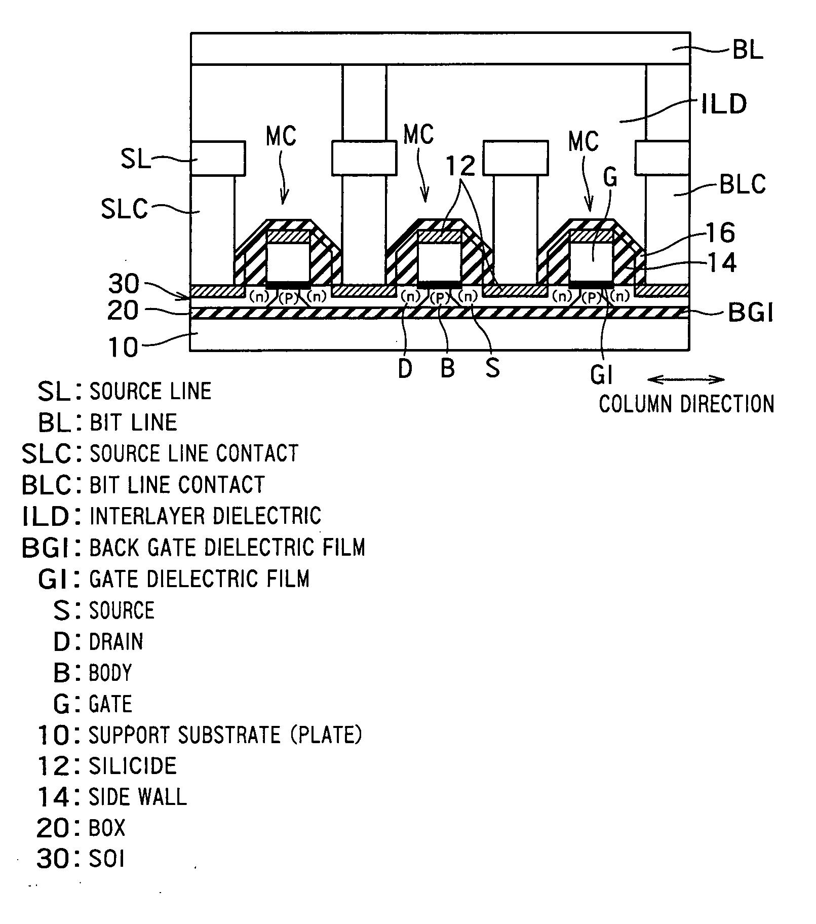
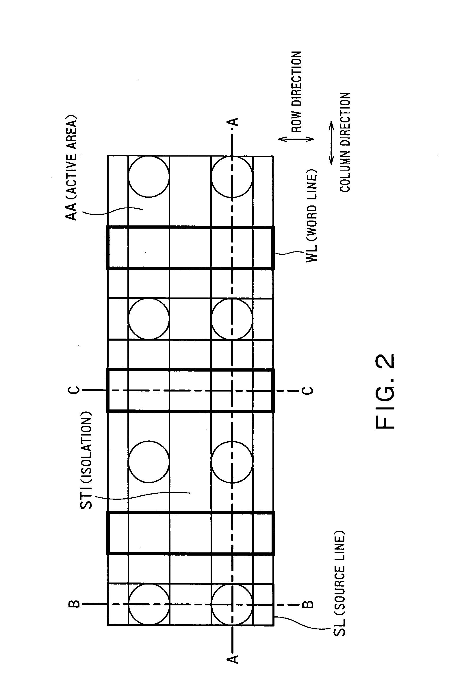
[0120]FIG. 11 is a plan view showing arrangement of wirings in an FBC memory device according to a third embodiment of the present invention. Bit lines BLs extend in the column direction. Word lines WLs and the source lines SLs extend in the row direction orthogonal to the bit lines BLs. Memory cells MCs are arranged at crosspoints between the bit lines BLs and the word lines WLs, respectively. Each of the bit lines BLs is connected to the drain D of each memory cell MC via a bit line contact BLC. The word lines WLs also function as the gate electrode G of each of the memory cells MCs. Each of the source lines SLs is connected to the source S of each memory cell MC via a source line contact SLC.
[0121]In view of a positional deviation between bit line contacts BLCs and the source line contacts SLCs, a margin between one word line WL and one bit line contact BLC and that between one word line WL and one source line contact SLC are set to a distance D. The distance D is gradually reduc...
PUM
 Abstract
Description
Claims
Application Information