

Lateral junction field-effect transistor
a field-effect transistor and lateral junction technology, applied in transistors, electrical devices, semiconductor devices, etc., to prevent leakage current generation and improve resistance to voltag
- Summary
- Abstract
- Description
- Claims
- Application Information
AI Technical Summary
Benefits of technology
Problems solved by technology
Method used
Image

Examples
first embodiment
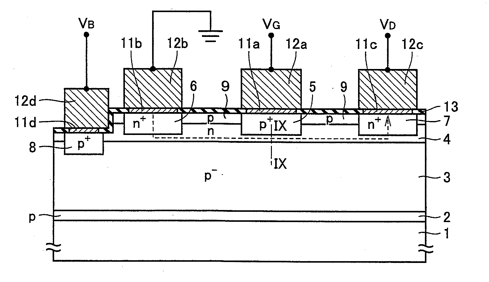
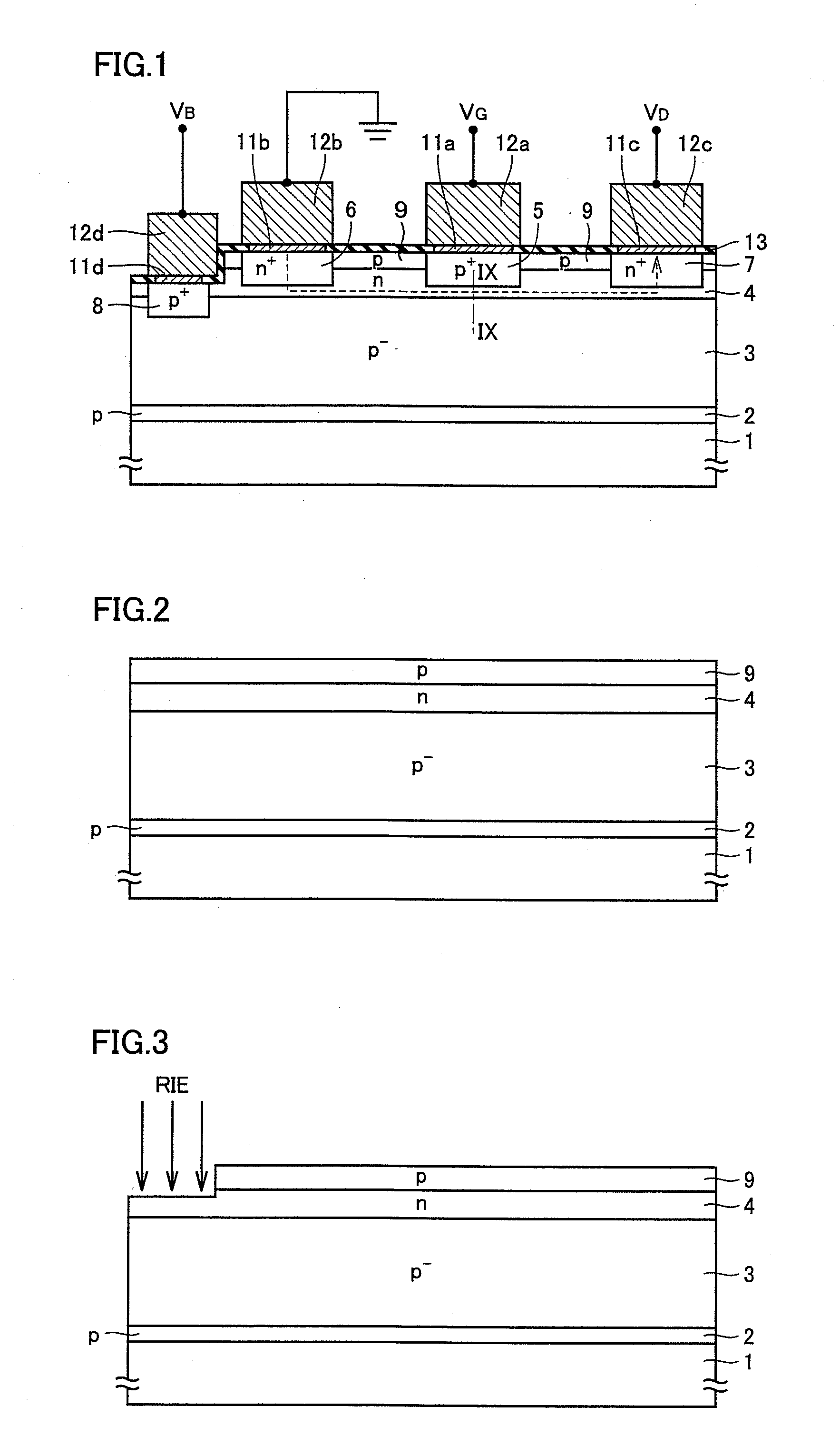
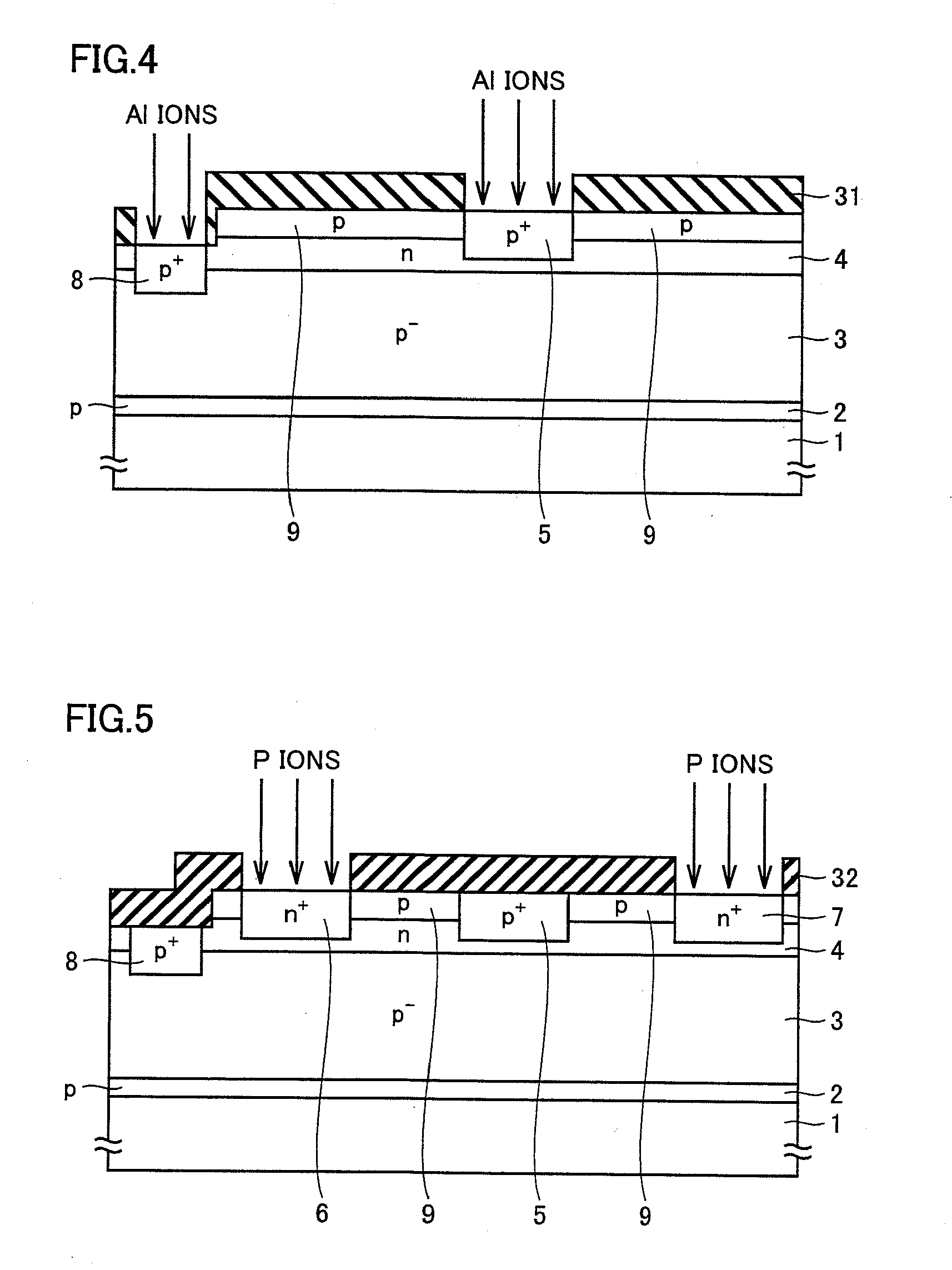
[0039]FIG. 1 is a cross section schematically showing a structure of a lateral junction field-effect transistor in a first embodiment of the present invention. Referring to FIG. 1, a single crystal substrate 1 that is of any conductivity type and made for example of 4H—SiC (silicon carbide) is used as a semiconductor substrate. On substrate 1, a p-type epitaxial layer 2 and a p− epitaxial layer (withstand voltage keeping region) 3 are formed in layers stacked in this order. P-type epitaxial layer 2 includes Al (aluminum) as a p-type impurity with a concentration for example of 5.0×1016 cm−3 and has a thickness for example of 0.5 μm. P− epitaxial layer 3 includes Al as a p-type impurity with a concentration for example of 1.0×1016 cm−3 and has a thickness for example of 10 μm.
[0040]On p− epitaxial layer 3, an n-type epitaxial layer (channel region) 4 is formed. N-type epitaxial layer 4 includes N (nitrogen) as an n-type impurity with a concentration for example of 2.0×1017 cm−3 and h...
second embodiment
[0061]FIG. 10 is a cross section schematically showing a structure of a lateral junction field-effect transistor in a second embodiment of the present invention. Referring to FIG. 10, the lateral junction field-effect transistor in the present embodiment differs from the structure of the first embodiment shown in FIG. 1 in that the former is configured to allow a gate potential VG to be applied to control electrode 12d. Therefore, control electrode 12d may be electrically connected to gate electrode 12a.
[0062]Components of the lateral junction field-effect transistor in the present embodiment other than the above-described one are substantially identical to those of the above-described structure of the first embodiment. Therefore, like components are denoted by like reference characters and the description thereof will not be repeated.
[0063]Further, a manufacturing method in the present embodiment is also substantially identical to the manufacturing method in the first embodiment. ...
PUM
 Abstract
Description
Claims
Application Information