Pulse width modulation circuit and liquid jet printing apparatus

Active Publication Date: 2010-04-22
SEIKO EPSON CORP
View PDF7 Cites 28 Cited by
  • Summary
  • Abstract
  • Description
  • Claims
  • Application Information

AI Technical Summary

Benefits of technology

[0025]According to this pulse width modulation circuit, it is possible to stabilize the pulse width modulated signal

Problems solved by technology

However, in the event of heightening the frequency of the clock signals which are the source, a calculation of a comparison between the reference signals and input signal cannot keep pace, making an internal calculation process unstable.
That is, there is a limit on a balance between a high resolution and a high speed response.
However, as a resister or switching element which connects or disconnects the outputs at each voltage stage is needed in order to output the multivalued signal in the voltage axis direction as in the pulse width modulation circuits described in JP-A-4-159821 and JP-A-2004-312442, a need occurs to install the resistor

Method used


Image

  • Pulse width modulation circuit and liquid jet printing apparatus
  • Pulse width modulation circuit and liquid jet printing apparatus
  • Pulse width modulation circuit and liquid jet printing apparatus

Examples


Example

[0064]FIG. 7 shows a first embodiment of the pulse width modulation circuit used as the previously described modulation circuit 26. With the pulse width modulation circuit, a clock signal generation circuit 31, by dividing or multiplying the clock signal CLK, and shifting the phases, generates first to fourth clock signals CLK1 to CLK4 with mutually differing phases, and first to fourth counters 32a to 32d count the clock signals CLK1 to CLK4, and output results of the count as first to fourth reference signals CNT1 to CNT4. The count increases or decreases by a predetermined value set in advance at each rise of the clock signals CLK1 to CLK4.

[0065]The reference signals CNT1 to CNT4 become sawtooth wave signals by configuring in such a way that the count increases by the predetermined value at each rise of the clock signals CLK1 to CLK4, and the count value is reset in the event that a predetermined time elapses, or the count value becomes a predetermined value or more. Meanwhile, t...

Example

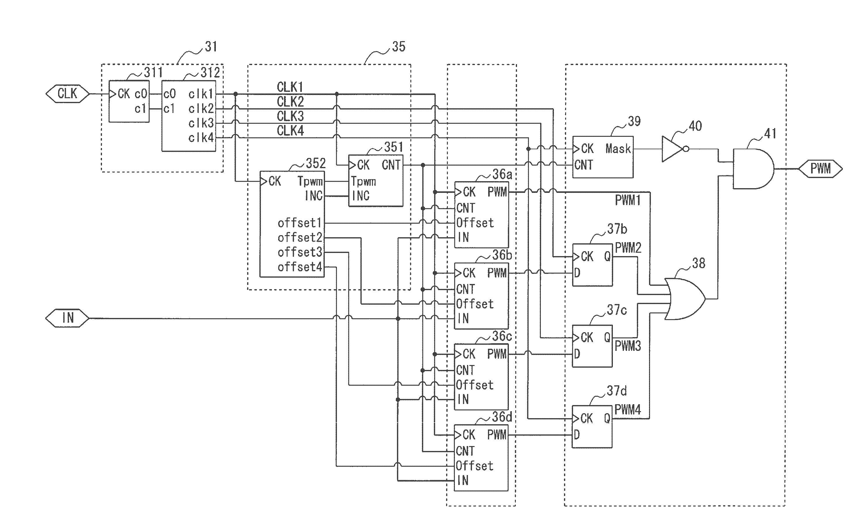
[0071]In the second embodiment, there is only one clock signal counter. A clock signal generation circuit 31 having a function equivalent to that of FIG. 7 is provided with a phase locked loop (PLL) circuit 311 which outputs clock signals, a frequency of which equals to the integral multiple of the frequency of the clock signals CLK, and a multiphase clock circuit 312 which outputs first to fourth clock signals CLK1 to CLK4 with phases shifted 90 degrees each, that is, with mutually differing phases, from the clock signals equal to the integral multiple. It is also acceptable to use a delay locked loop (DLL) circuit in place of the PLL circuit.

[0072]The counter circuit 35 counts only the first clock signal CLK1, among the clock signals CLK1 to CLK4, using the counter 351, and outputs a voltage signal in accordance with the count value as the reference signal CNT. The counter circuit 35 is provided with a pulse width modulation management circuit 352 which gives increase start initia...

Example

[0081]FIG. 10 is a block diagram showing a third embodiment of the pulse width modulation circuit of some aspects of the invention. In the third embodiment too, although the diagram is also divided into blocks, actually, it is also acceptable to construct it with the computation process using the program. In FIG. 10, a clock signal generation circuit 31, having the same functions as those of the first embodiment and second embodiment, generates first to fourth clock signals CLK1 to CLK4 with mutually differing phases, specifically, with phases shifted 90 degrees each, from the previously described clock signal CLK.

[0082]Among first to fourth registers 42a to 42d which read an input signal IN, in this case, a drive waveform signal WCOM, the first register 42a reads the input signal IN at a rise of a fourth clock signal CLK4, the second register 42b reads the input signal IN at a rise of a first clock signal CLK1, the third register 42c reads the input signal IN at a rise of a second ...


PUM


Abstract

A pulse width modulation circuit includes: a reference signal generator which generates a plurality of mutually differing reference signals; a comparator which compares the reference signals and an input signal with respect to magnitude, and outputs results of the comparison as a plurality of comparison signals with mutually differing phases; and a synthesizer which, using a logical operation, outputs the plurality of comparison signals output from the comparator as a pulse width modulated signal configured of one or more binary signals.

Description

[0001]This application claims priority to Japanese Patent Application No. 2008-271962 filed on Oct. 22, 2008, and the entire disclosure thereof is incorporated herein by reference.BACKGROUND[0002]1. Technical Field[0003]The present invention relates to a pulse width modulation circuit which modulates an input signal, and outputs a binary, pulse width modulated signal.[0004]2. Related Art[0005]A pulse width modulation circuit which modulates a pulse of an input signal, and outputs a binary, pulse width modulated signal, is widely used to digitally control a voltage. With the pulse width modulation circuit, reference signals with a sawtooth wave, triangle wave, or the like responding to clock signals are generated, the reference signal and the input signal are compared with respect to magnitude, and a binary voltage signal which is at a high level when the input signal is larger than the reference signals, and at a low level when the input signal is smaller than the reference signals,...

Claims


Application Information

Patent Timeline
IPC IPC(8): H03K7/08
CPCH03K5/15013H03K2005/00247H03K7/08B41J2/04541B41J2/04581B41J2/04588B41J2/04593B41J2/04596
Inventor MIYAZAKI, SHINICHIYOSHINO, HIROYUKIAZAMI, NOBUAKIOSHIMA, ATSUSHIIDE, NORITAKATABATA, KUNIO
Owner SEIKO EPSON CORP
Why Eureka
Try Eureka