High intensity, strobed led micro-strip for microfilm imaging system and methods

a microfilm imaging and led microstrip technology, applied in the field of microfilm imaging systems, can solve the problems of limiting the exposure illumination required for full speed operation, relatively expensive broadband color correction lenses, and low efficiency of camera speed, and achieves high efficiency, no meaningful ir emissions, and high illumination intensity. high uniform

Inactive Publication Date: 2010-04-22
BREISH KURT +2
View PDF100 Cites 11 Cited by
  • Summary
  • Abstract
  • Description
  • Claims
  • Application Information

AI Technical Summary

Benefits of technology

[0010]An advantage of the present invention is that the light source is highly efficient in that the light strip produces a narrow-band emission spectrum that is closely matched to the sensitivity band of the CCD elements. Spectrum filtering, and associated loss of light power, is not required. Further, the light strip produces no meaningful IR emissions. Any generated IR is too attenuated to reach and affect the CCD imager. An IR filter is not required.
[0011]Another advantage of the present invention is that the light source can be strobed synchronous with the exposure period of the CCD imager. The illumination cycle edges are sharp with repeatable characteristics and the illumination intensity is highly uniform. The intensity level can be set to different specific levels, enabling adaptation to different operating factors including media transport speed, desired imaging resolution, contrast range, and various aspects of a specific microfilm media. The power requirements and heat-generation by the light source are therefore minimized in alignment with the specific illumination needs of the imager.
[0012]A further advantage of the present invention is that a higher specific illumination intensity is achieved during the required duration of an imager exposure cycle. Higher specific illumination enables a reduction in the required exposure duty cycle and a corresponding increase in image resolution along the media transport axis. Narrow band illumination of the media also reduces light contributions from effectively adjacent image lines, thereby reducing line blending and further increasing effective imager resolution along the media transport axis. Collectively, up to a two-fold resolution improvement, relative to conventional systems, may be realized. Image resolution improvement in both the transport and transverse axises is also obtained as a result of the reduced color spectrum refraction variance due to the substantially monochromatic spectrum of the source light strip. The manufactured cost of the lens is also reduced.
[0013]Still another advantage of the present invention is that the light source is structurally stable and that the LED micro-strip is aligned and physically matches the CCD imager configuration. The mechanically fixed structure of the LED micro-strip results in less sensitivity to vibration, particularly relative to an incandescent filament. The fixed, multiple emitter element array structure of the LED micro-strip and associated diffuser element improves the quality of light dispersion and avoids the potential for hot or cold illumination spots. The narrow cross section of the LED micro-strip enables the efficient projection of illumination through the active area of the microfilm and on to the CCD imager.
[0014]Yet another advantage of the present invention is that the light source substantially improves the controlled delivery of narrow width illumination to the diffuser and further maintains a narrow width delivery of the randomized illumination to and through the microfilm. An optional, generally preferred, cylindrical lens is placed in the optical path to efficiently concentrate narrow width illumination onto the diffuser element. A narrow reflective channel is provided to restrain illumination dispersal from the diffuser while additionally allowing the diffuser to be placed outside of the maximum depth of field of the lens observable by the camera.
[0015]A still further advantage of the present invention is that the LED light source is constructed as a compact unitized structure containing a fully solid-state active light emitter. The light source structure includes an integral heat sink well sufficient to avoid any thermal distortion of the LED micro-strip. The combined use of solid-state emitters and strobed control results in power consumption and heat generation levels that are one-tenth that of conventional incandescent light sources. The solid-state LED micro-strip has a rated mean-time-between-failure of more than about 50 times that of conventional incandescent light sources. While not expected to fail within the normal operating lifetime of a microfilm scanner system, the light source is a readily serviceable and maintainable component.

Problems solved by technology

A principal limiting factor on camera speed is the exposure illumination required for full speed operation.
Broadband color corrected lenses are, unfortunately, relatively expensive.

Method used


Image

  • High intensity, strobed led micro-strip for microfilm imaging system and methods
  • High intensity, strobed led micro-strip for microfilm imaging system and methods
  • High intensity, strobed led micro-strip for microfilm imaging system and methods

Examples


Embodiment Construction

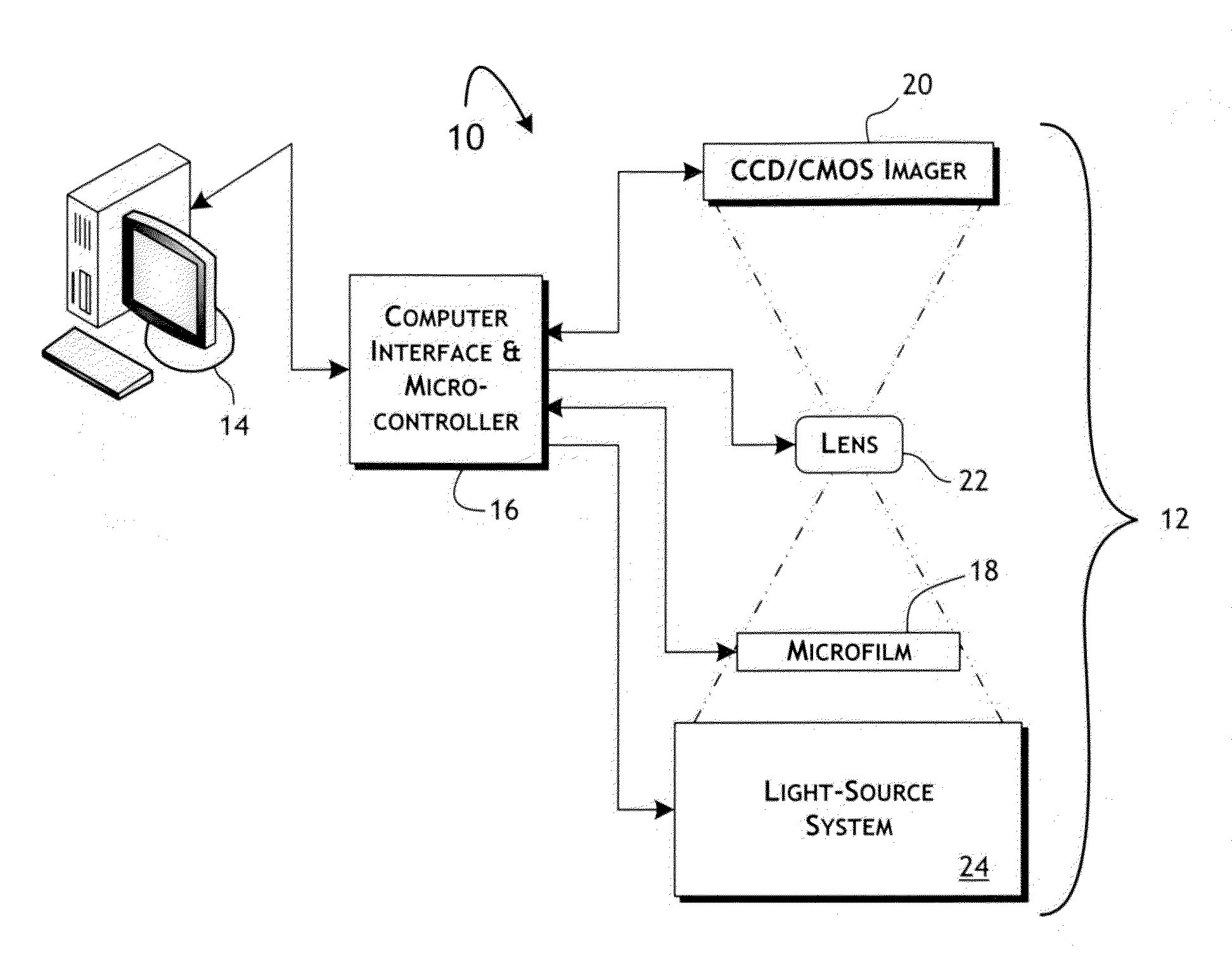
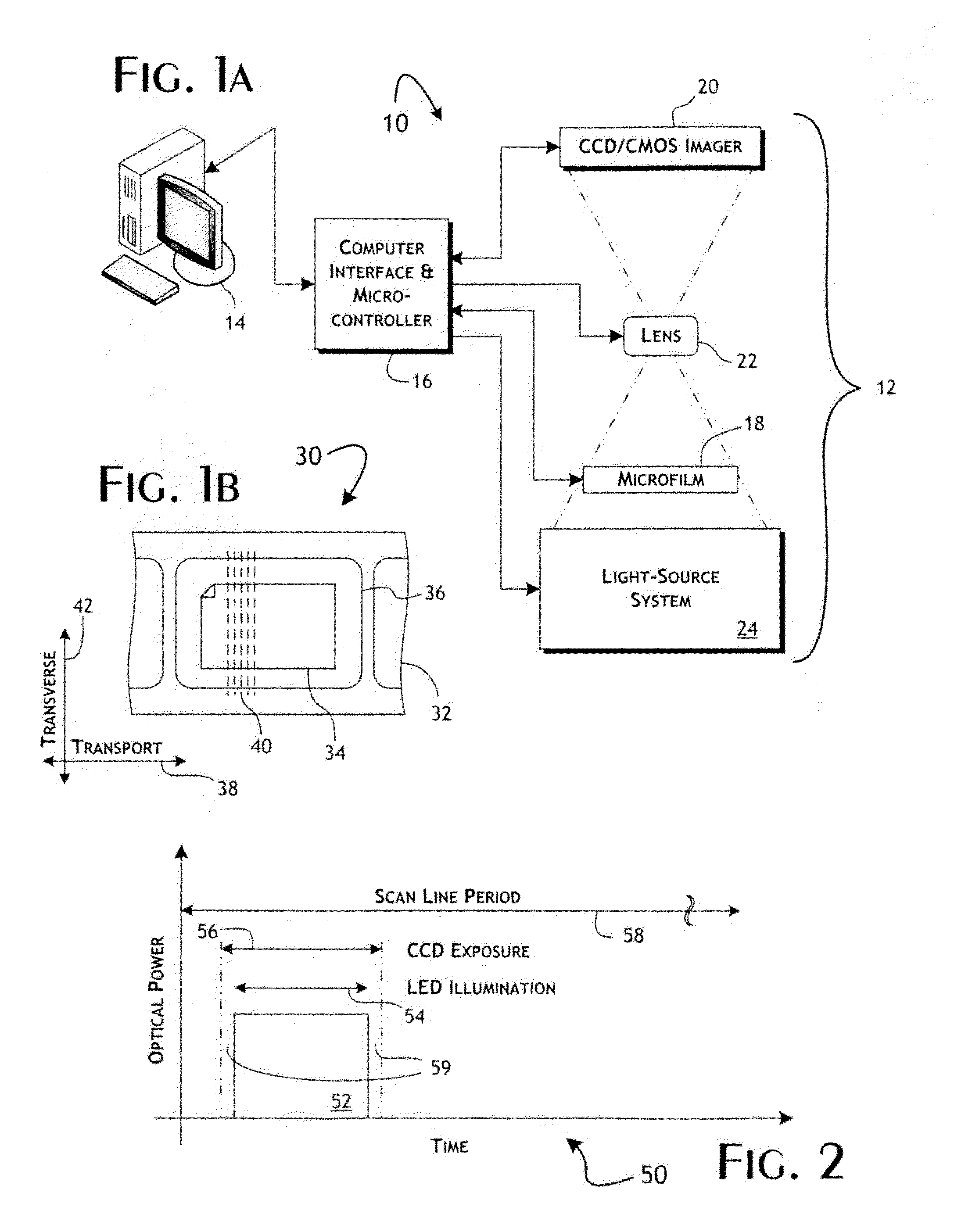
[0029]The present invention provides a high-intensity, strobed light source appropriate for use in high-speed scan imaging systems, such as the continuous scan microfilm imaging system 10 shown in FIG. 1A. The imaging system 10 preferably includes an optomechanical imaging system 12, an imaging system management computer 14, and a microprocessor-based controller 16 suitable for real-time control applications. The imaging system 12 preferably includes a continuous microfilm media transport system 18, a line scan-type CCD or CMOS imaging camera, or imager, and objective lens 22. A preferred mechanical system configuration, including feedback managed speed controller, is described in High-Speed Continuous Linear Film Transport System, U.S. Pat. No. 7,093,939 issued Aug. 22, 2006 to Breish et al., and which is hereby incorporated by reference. The light source 24 of the present invention is positioned to project a high-intensity light beam through the microfilm media to the imager 20, s...


PUM


Abstract

A light source, suitable for use in a high-speed, continuous transport microfilm imaging system, includes an LED emitter element thermally coupled to a heat sink and is mounted within a light source housing. A light output opening in the light source housing, further defined by a narrow width light transfer channel, defines a narrow width active illumination area on the microfilm media. An optical diffusion plate, providing for a randomized directional distribution of light emitted by the LED emitter element, is mounted within the light source housing in an optical path extending between the light output opening and the LED emitter element. A switched current source is coupled to the LED emitter element to enable strobed operation synchronous with the periodic operation of a line imaging camera. The LED emitter element can be construed as a linear micro-strip array of LED elements. A cylindrical lens can be place in the optical path between the LED emitter element and diffusion plate to narrow and increase the intensity of light incident on and transmitted through the diffusion plate.

Description

BACKGROUND OF THE INVENTION[0001]1. Field of the Invention[0002]The present invention is generally related to microfilm imaging systems and, in particular, to a high-speed microfilm imaging system utilizing a compact, high-intensity LED micro-strip light source strobed synchronous with a line-scan imaging camera.[0003]2. Description of the Related Art[0004]Microfilm imaging systems are conventionally used for the high-speed transfer of microfilm documents in existing library archives to a digital image format. Existing microfilm scanning systems implement various film media transport systems and utilize high capture rate digital cameras. Rather than image an entire two-dimensional frame at a time, some microfilm imaging systems implement a continuous motion transport system and image a series of one-dimensional line exposures typically oriented transverse to the media transfer path. The line exposures are captured and transferred into data buffers for processing, typically by a digi...

Claims


Application Information

Patent Timeline
Patent Type & Authority Applications(United States)
IPC IPC(8): G03B15/03H05B41/36F21V11/00
CPCG03B15/03
Inventor BREISH, KURTSAND, DENNIS R.WREDE, JEFFREY A.
Owner BREISH KURT
Why Eureka
Try Eureka