

Oxide semiconductor, thin film transistor, and display device
a thin film transistor and semiconductor technology, applied in the direction of transistors, semiconductor devices, electrical appliances, etc., can solve the problems of not being able to be of normal-off type, thin film transistors have no advantage of being used as driving elements of display panels, etc., to achieve the effect of reducing the off current of the thin film transistor, reducing the defects of the oxide semiconductor, and increasing the on-off ratio
- Summary
- Abstract
- Description
- Claims
- Application Information
AI Technical Summary
Benefits of technology
Problems solved by technology
Method used
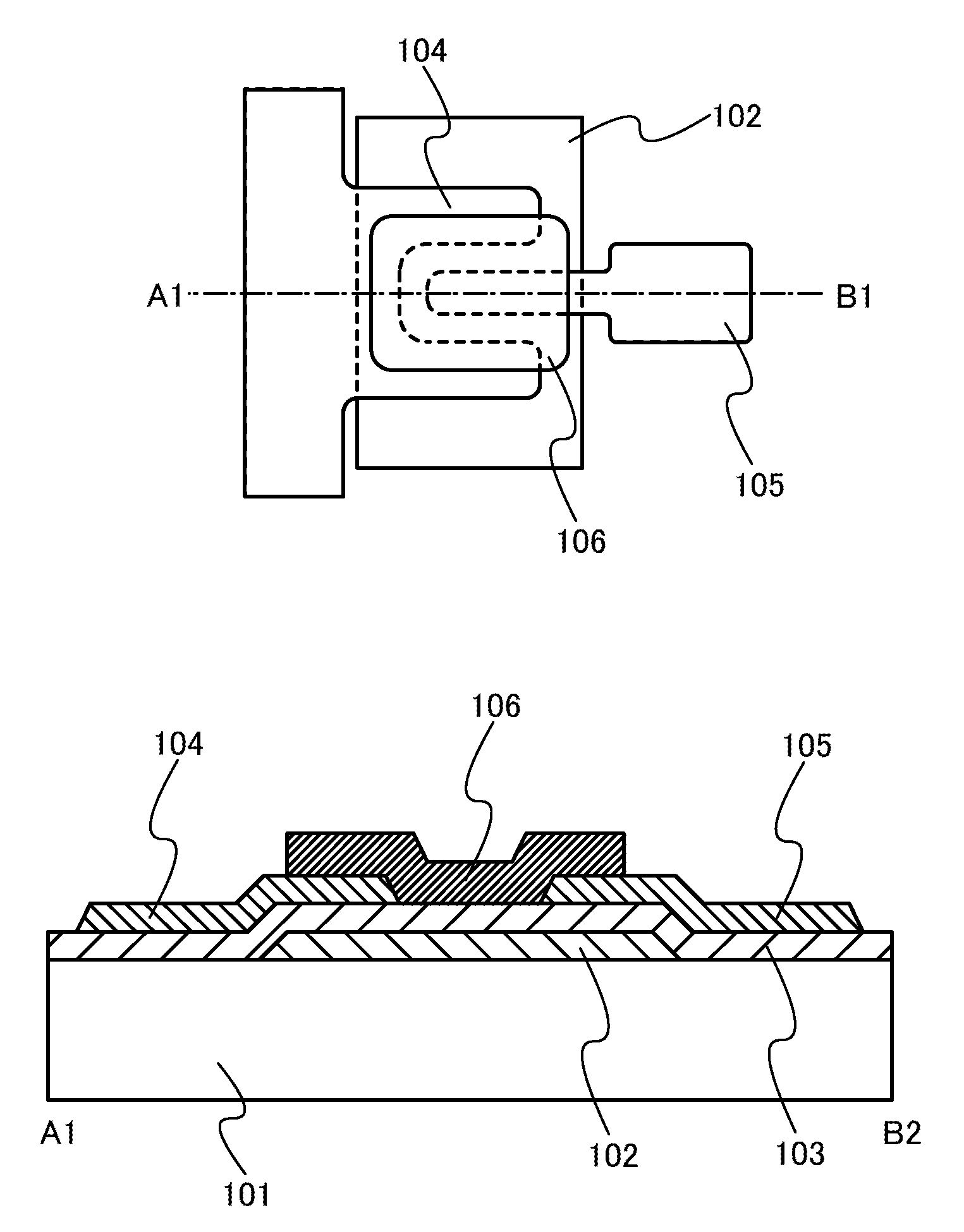
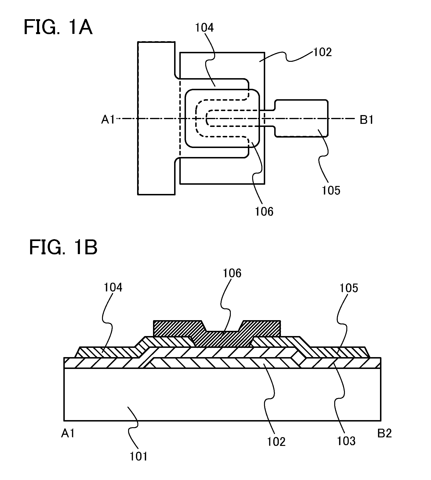
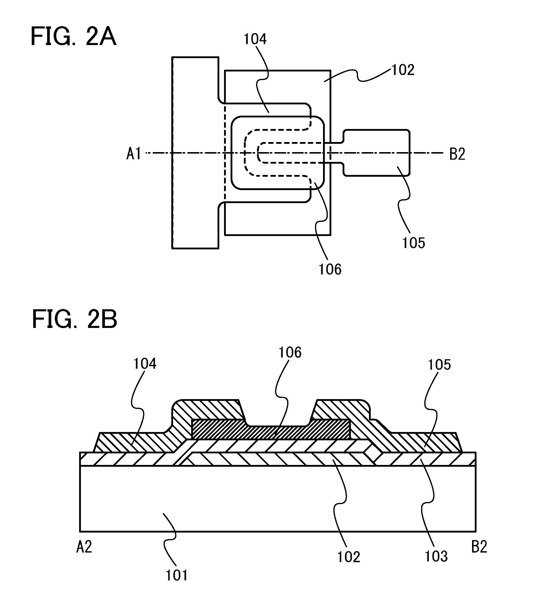
Image

Examples
example 1
(Composition of Oxide Semiconductor Film)
[0128]Oxide semiconductor films were formed over glass substrates by a sputtering method under the conditions described below.
(Condition 1)
[0129]Target composition: In2O3:Ga2O3:ZnO=1:1:1[0130](In:Ga:Zn=1:1:0.5)[0131]Ar gas flow rate: 40 sccm[0132]Pressure: 0.4 Pa[0133]Electric power (DC): 500 W[0134]Substrate temperature: room temperature
(Condition 2)
[0135]Target composition: In2O3:Ga2O3:ZnO=1:1:1[0136](In:Ga:Zn=1:1:0.5)[0137]Ar gas flow rate: 10 sccm[0138]Oxygen gas flow rate: 5 sccm[0139]Pressure: 0.4 Pa[0140]Electric power (DC): 500 W[0141]Substrate temperature: room temperature
[0142]Table 1 shows the typical results of the quantification of the oxide semiconductor films formed under the above conditions, which was performed by Rutherford backscattering spectrometry (RBS).
TABLE 1Composition (atomic %)InGaZnOArComposition formulaCondition 11715.87.559.40.3InGa0.93Zn0.44O3.49Condition 21614.77.261.70.4InGa0.92Zn0.45O3.86
[0143]According to th...
PUM
 Abstract
Description
Claims
Application Information