Semicoductor device

Active Publication Date: 2010-04-29
ROHM CO LTD
View PDF10 Cites 3 Cited by
  • Summary
  • Abstract
  • Description
  • Claims
  • Application Information

AI Technical Summary

Benefits of technology

[0008]It is therefore an object of the present invention to provide a semiconductor device including a MOS transistor which has a higher breakdown voltage and a higher ESD resistance, and can be easily mounted together with other type of MOS transistor.Means for Solving the Problems
[0011]In a MOS transistor including the source region, the drain region, the gate insulation film and the gate electrode, the drain region and the gate insulation film are spaced from each other, whereby an electric field generated between the drain region and the gate insulation film is weakened. This prevents the field concentration from occurring in the vicinity of the drain region, thereby preventing the breakdown of the gate insulation film which may otherwise occur due to the field concentration. Therefore, even if the thickness of the gate insulation film is reduced, the MOS transistor has a higher breakdown voltage. In addition, the reduction in the thickness of the gate insulation film reduces ON-resistance. As a result, it is possible to achieve improvement in the breakdown voltage of the MOS transistor as well as the reduction in ON-resistance.
[0013]Further, the MOS transistor including the source region, the drain region, the gate insulation film and the gate electrode is of a planar type and, therefore, can be easily mounted together with other planar type of MOS transistor on the same semiconductor substrate.
[0015]Where the device isolation trench is provided, the drain-gate isolation portion is preferably formed by filling a trench having the same depth as that of the device isolation portion from the surface of the semiconductor layer with the same dielectric as the device isolation portion. With this arrangement, the drain-gate isolation portion and the device isolation portion can be formed in the same step. As a result, a production process can be simplified.

Problems solved by technology

Therefore, where the DMOSFET and the MOSFET are to be mounted on the same semiconductor substrate, a process for fabricating the DMOSFET and the MOSFET is significantly complicated.
The DMOSFET also suffers from ESD breakdown of its gate oxide film, because the gate oxide film contacts an epitaxial layer serving as a drain region.

Method used


Image

  • Semicoductor device
  • Semicoductor device
  • Semicoductor device

Examples


Embodiment Construction

[0029]Embodiments of the present invention will hereinafter be described in detail with reference to the attached drawings.

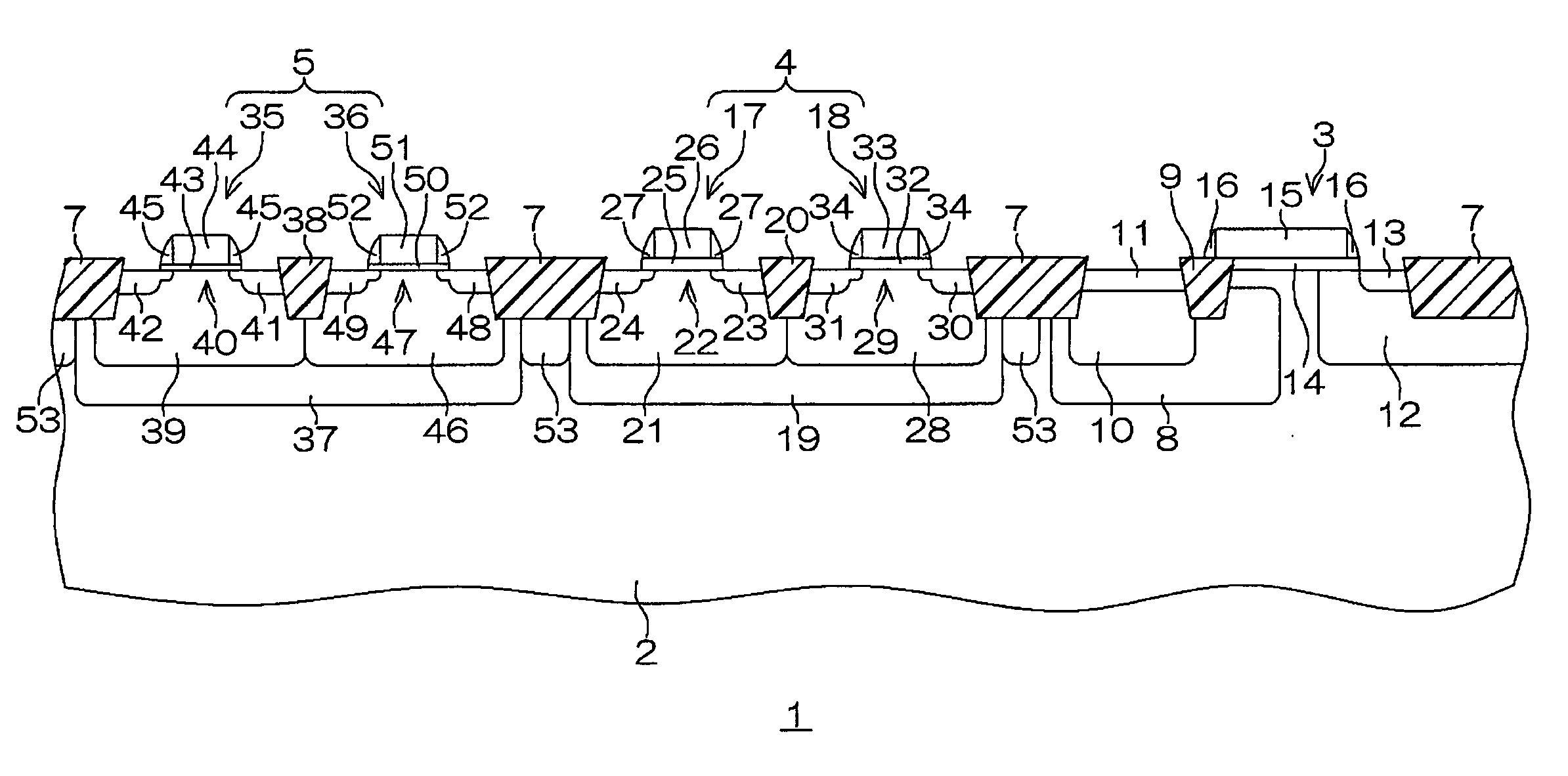
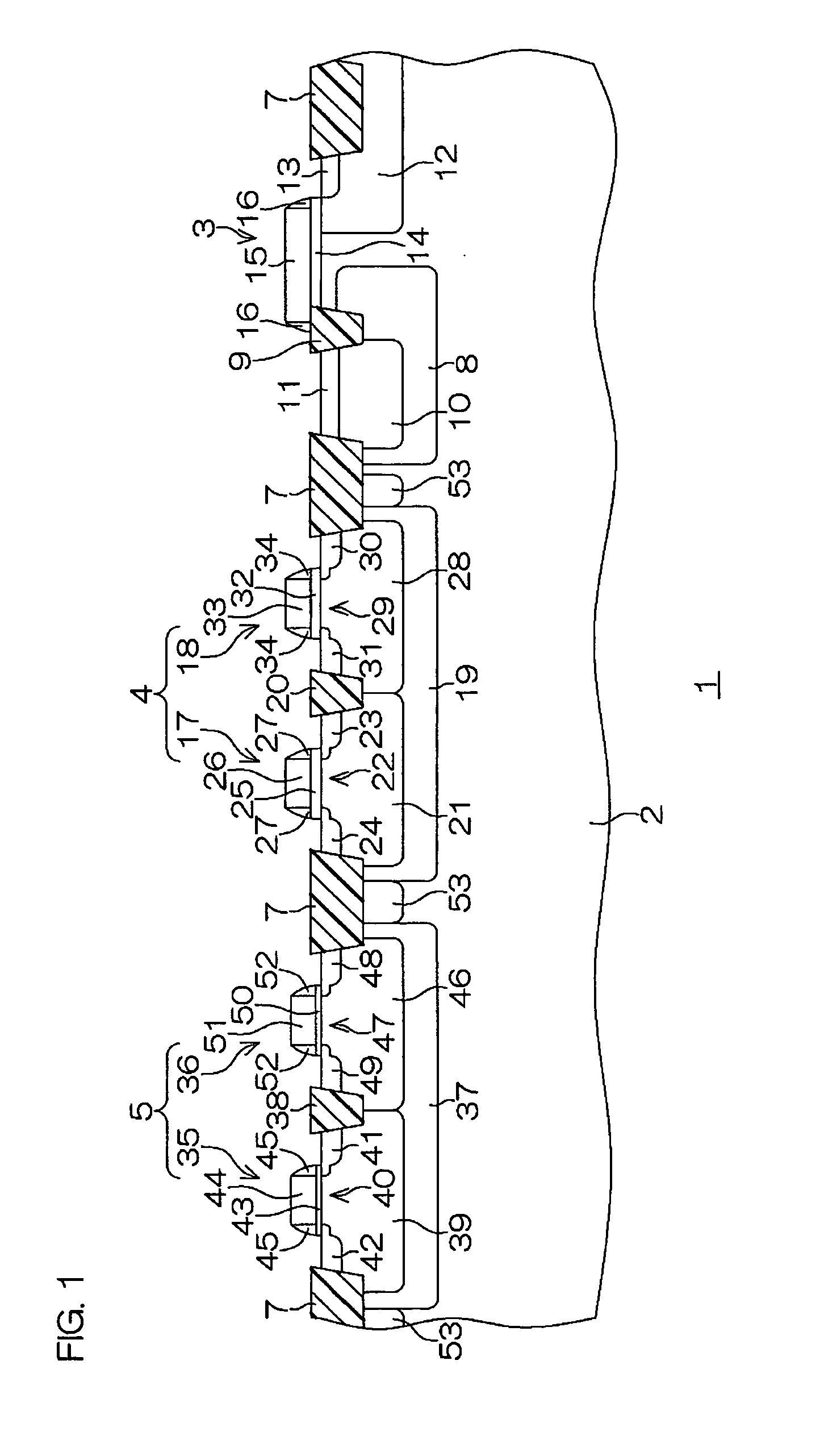
[0030]FIG. 1 is a schematic sectional view showing the construction of a semiconductor device according to one embodiment of the present invention.

[0031]The semiconductor device 1 includes an HVNMOSFET (high breakdown voltage NMOSFET) 3, an MVCMOSFET (medium breakdown voltage CMOSFET) 4 and an LVCMOSFET (low breakdown voltage CMOSFET) 5 provided on a P-type semiconductor substrate (e.g., a silicon substrate) 2.

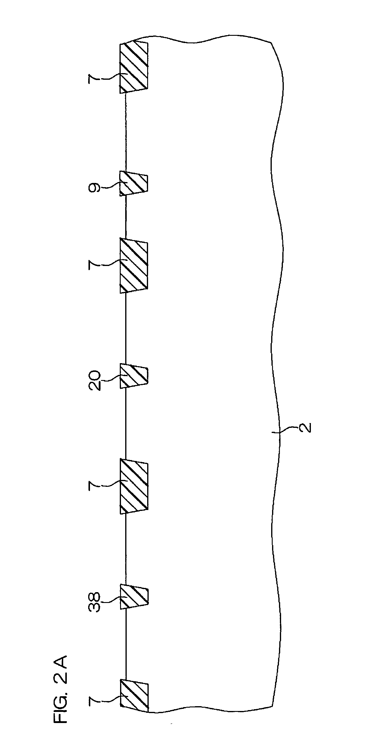
[0032]A device isolation portion 7 is provided in a surface layer portion of the semiconductor substrate 2 for isolating the HVNMOSFET 3, the MVCMOSFET 4 and the LVCMOSFET 5 from each other. Rectangular regions respectively formed with the HVNMOSFET 3, the MVCMOSFET 4 and the LVCMOSFET 5 are defined by the device isolation portion 7. The device isolation portion 7 has a structure such that a relatively shallow trench (e.g., having a depth of 0.2 to 0.5 μm ...


PUM


Abstract

An inventive semiconductor device includes a semiconductor layer, a source region provided in a surface layer portion of the semiconductor layer, a drain region provided in the surface of the semiconductor layer in spaced relation from the source region, a gate insulation film provided in opposed relation to a portion of the surface of the semiconductor layer present between the source region and the drain region, a gate electrode provided on the gate insulation film, and a drain-gate isolation portion provided between the drain region and the gate insulation film for isolating the drain region and the gate insulation film from each other in non-contact relation.

Description

TECHNICAL FIELD[0001]The present invention relates to a semiconductor device having a MOS transistor.BACKGROUND ART[0002]Semiconductor devices having an integrated circuit (driver IC) for driving a liquid crystal display panel, for example, are often configured such that plural types of MOSFETs (metal oxide semiconductor field effect transistors) having different breakdown voltages are mounted on a semiconductor substrate.[0003]FIG. 4 is a sectional view showing the basic construction of such a MOSFET.[0004]The MOSFET includes, for example, a source region 103 and a drain region 104 provided on opposite sides of a channel region 102 in a surface of a silicon substrate 101. A gate oxide film 105 of SiO2 (silicon oxide) is provided on the channel region 102 as extending between the source region 103 and the drain region 104. A gate electrode 106 of polysilicon is provided on the gate oxide film 105.[0005]The MOSFET having such a construction has a lower breakdown voltage on the order ...

Claims


Application Information

Patent Timeline
IPC IPC(8): H01L27/092H01L29/78
CPCH01L21/823814H01L21/82385H01L21/823857H01L21/823892H01L27/0922H01L27/0928H01L27/092H01L29/0847H01L29/1045H01L29/66659H01L29/7833H01L29/7835H01L27/088H01L29/0653
Inventor KOJIMA, MITSUO
Owner ROHM CO LTD
Why Eureka
Try Eureka