Method and apparatus for fabricating piezoresistive polysilicon by low-temperature metal induced crystallization

a piezoresistive polysilicon and low-temperature metal technology, applied in the field of semiconductor processing and devices, can solve the problems of low thermal budget of flexible substrates, dictating low-temperature processing, temperature too high to be used with flexible polyimide substrates, film contamination and uniformity, etc., and achieve excellent piezoresistive characteristics

Inactive Publication Date: 2010-04-29
BOARD OF RGT THE UNIV OF TEXAS SYST
View PDF7 Cites 39 Cited by
  • Summary
  • Abstract
  • Description
  • Claims
  • Application Information

AI Technical Summary

Benefits of technology

[0023]The present invention describes a low temperature method for fabricating silicon piezoresistors using aluminum induced crystallization (AIC). The processing technique of the present invention causes an amorphous silicon thin film to form crystalline grains in a short time period without resorting to high-temperature annealing,

Problems solved by technology

One challenge in fabricating sensors on flexible substrates is the low thermal budget of the flexible substrates, dictating low temperature processing.
These temperatures are too high to be used with flexible polyimide substrates.
However, this technique has issues with film contamination and uniformity when trying to deposit over large surfaces.
Single crystal diamond shows a very high GF of 2000 but for most applications it is prohibitively expensive.
However, due to thermal budget restrictions of the flexible substrate material, polysilicon films deposited by LPCVD can not be used.
This condition also restricts the use of PECVD for deposition of polysilicon on flexible substrate.
Although this technique is compatible with low-temperature substra

Method used


Image

  • Method and apparatus for fabricating piezoresistive polysilicon by low-temperature metal induced crystallization
  • Method and apparatus for fabricating piezoresistive polysilicon by low-temperature metal induced crystallization
  • Method and apparatus for fabricating piezoresistive polysilicon by low-temperature metal induced crystallization

Examples


Embodiment Construction

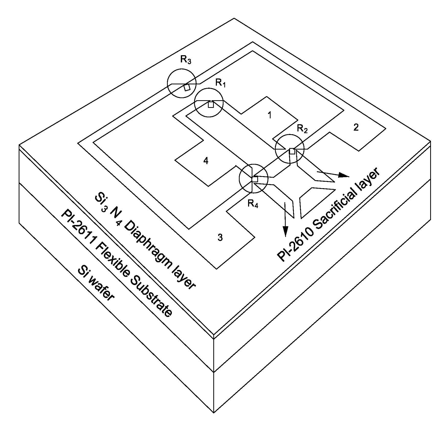
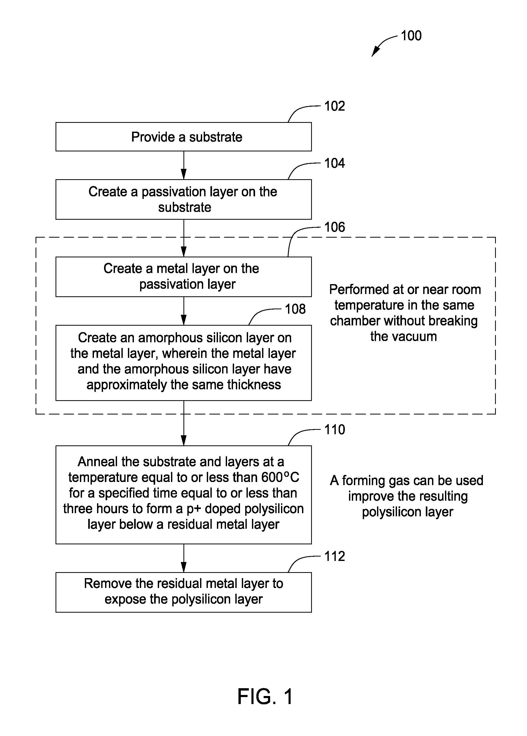
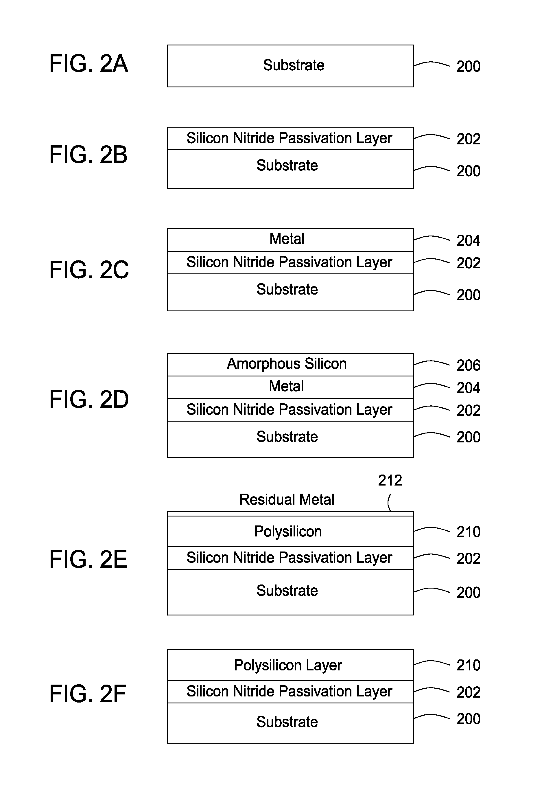
[0059]While the making and using of various embodiments of the present invention are discussed in detail below, it should be appreciated that the present invention provides many applicable inventive concepts that can be embodied in a wide variety of specific contexts. The specific embodiments discussed herein are merely illustrative of specific ways to make and use the invention and do not delimit the scope of the invention. The discussion herein relates primarily to low-temperature aluminum induced crystallization and polysilicon piezoresistive pressure sensors, but it will be understood that the concepts of the present invention are applicable to any low-temperature metal induced crystallization and any semiconductor device that can benefit from the use of a piezoresistive polysilicon film.

[0060]To facilitate the understanding of this invention, a number of terms are defined below. Terms defined herein have meanings as commonly understood by a person of ordinary skill in the areas...


PUM


Abstract

The present invention provides a method and apparatus for fabricating piezoresistive polysilicon on a substrate by low-temperature metal induced crystallization by: (1) providing the substrate having a passivation layer; (2) performing, at or near room temperature in a chamber without breaking a vacuum or near-vacuum within the chamber, the steps of: (a) creating a metal layer on the passivation layer, and (b) creating an amorphous silicon layer on the metal layer, wherein the metal layer and the amorphous silicon layer have approximately the same thickness; (3) annealing the substrate, the passivation layer, the metal layer and the amorphous silicon layer at a temperature equal to or less than 600° C. and a period of time equal to or less than three hours to form a doped polysilicon layer below a residual metal layer; and (4) removing the residual metal layer to expose the doped polysilicon layer.

Description

CROSS-REFERENCE TO RELATED APPLICATIONS[0001]This application claims benefit of U.S. Provisional application Ser. No. 61 / 088,820 filed on Aug. 14, 2008 which is incorporated herein by reference in its entirety.STATEMENT OF FEDERALLY FUNDED RESEARCH[0002]This invention was made with U.S. Government support under Contract Nos. ECS-0401148 and FA9550-06-1-0413 awarded by the NSF and the Air Force Office of Scientific Research (AFOSR), respectively. The government has certain rights in this invention.FIELD OF THE INVENTION[0003]The present invention relates generally to the field of semiconductor processing and devices and, more particularly, to a method and apparatus for fabricating piezoresistive polysilicon by low-temperature metal induced crystallization.BACKGROUND OF THE INVENTION[0004]Without limiting the scope of the invention, its background is described in connection with the deposition of silicon films by aluminum induced crystallization.[0005]Recently there has been an increa...

Claims


Application Information

Patent Timeline
IPC IPC(8): H01L29/84H01L21/28H01L21/30
CPCG01L9/0042G01L9/0054H01L21/0237H01L21/02488H01L21/02491H01L41/25H01L21/02672H01L21/324H01L41/1132H01L41/1138H01L21/02532H01L21/3247H10N30/03H10N30/302H10N30/308
Inventor CELIK-BUTLER, ZEYNEPPATIL, SURAJ K.BUTLER, DONALD PHILIP
Owner BOARD OF RGT THE UNIV OF TEXAS SYST
Why Eureka
Try Eureka