Optoelectronic device based on non-polar and semi-polar aluminum indium nitride and aluminum indium gallium nitride alloys

a technology of aluminum indium nitride and optoelectronic devices, which is applied in semiconductor devices, lasers, semiconductor lasers, etc., can solve the problems of low material quality, low power and high-efficiency leds and lds in the deep uv (duv) region of the spectrum, and not been achieved

Active Publication Date: 2010-05-06
RGT UNIV OF CALIFORNIA
View PDF8 Cites 140 Cited by
  • Summary
  • Abstract
  • Description
  • Claims
  • Application Information

AI Technical Summary

Benefits of technology

[0017]For example, a light emitting device may comprise (a) an AlxIn1-xN or AlyInzGa1-y-zN based n-type cladding layer on the non-polar or semi-polar GaN substrate; (b) the one or more light emitting layers comprising an AlxIn1-xN or AlyInzGa1-y-zN based single quantum well (SQW) or multiple quantum well (MQW) on the n-type cladding layers; (c) one or more AlxIn1-xN or AlyInzGa1-y-zN based electron blocking layers on the quantum well layers; and (d) an AlxIn1-xN or AlyInzGa1-y-zN based p-type cladding layer on the electron blocking layers, (e) wherein the AlxIn1-xN or AlyInzGa1-y-zN layers are non-polar or semi-polar.
[0018]In another example, the optoelectronic device may comprise (a) an first (Al,In,Ga)N layer having a first conductivity type; (b) a second (Al,In,Ga)N layer having a second conductivity type; and (c) an (Al,In,Ga)N quantum-well structure comprising an (Al,In,Ga)N quantum well layer epitaxially on a non-polar or semi-polar plane of a first (Al,In,Ga)N quantum well barrier layer, and a second (Al,In,Ga)N quantum well barrier layer epitaxially on a non-polar or semi-polar plane of the (Al,In,Ga)N quantum well layer, wherein (1) the quantum well structure is epitaxially on a non-polar or semi-polar plane of the first (Al,In,Ga)N layer such that the (Al,In,Ga)N quantum well structure is between the first (Al,In,Ga)N layer and the second (Al,In,Ga)N layer, and (2) the quantum well has a thickness and (Al,In,Ga)N composition that emits electroluminescence having a peak wavelength less than 360 nanometers (nm). For example, the light emitting device may have a peak emission wavelength ranging from 280 nm to 360 nm.
[0019]The (Al,In,Ga)N quantum well structure may be epitaxially on an (Al,In,Ga)N layer, wherein the (Al,In,Ga)N layer has a dislocation density of an (Al,In,Ga)N layer that is grown epitaxially on, and closely lattice matched to, GaN. For example, the dislocation density may be less than 106 cm−2, which is the dislocation density expected from an underlying GaN substrate, and the (Al,In,Ga)N layer does not comprise a lateral epitaxial overgrowth. For example, “closely lattice-matched” is close enough that there is no relaxation of the film at the thicknesses grown. No relaxation means no more than the dislocations from the substrate.
[0020]The light emitting device may further comprise the (Al,In,Ga)N quantum well structure epitaxially on a non-polar or semi-polar plane of an (Al,In,Ga)N layer; and a dislocation density of the (Al,In,Ga)N layer that is sufficiently low, wherein the non-polar or semi-po

Problems solved by technology

However, high-power and high-efficient LEDs and LDs in the deep UV (DUV) region of the spectrum (emitting light with less than roughly 360 nm wavelengths) have not been achieved due to the difficulties in the growth, and thus poor material quality, and the absence of a bulk aluminum nitride (AlN) substrate.
Because of this heteroepitaxial growth, AlN or AlGaN buffer layers bear a dislocation density on the order of 1010 cm−2, and the dislocations propagate through the subsequent layers, resulting in poor material quality.
In contrast, AlGaN-based devices are sensitive to the dislocation density due to the absence of the indium clustering, and therefore the performance of AlGaN-based devices is directly affected by the number

Method used


Image

  • Optoelectronic device based on non-polar and semi-polar aluminum indium nitride and aluminum indium gallium nitride alloys
  • Optoelectronic device based on non-polar and semi-polar aluminum indium nitride and aluminum indium gallium nitride alloys
  • Optoelectronic device based on non-polar and semi-polar aluminum indium nitride and aluminum indium gallium nitride alloys

Examples


Embodiment Construction

[0027]In the following description of the preferred embodiment, reference is made to the accompanying drawings which form a part hereof, and in which is shown by way of illustration a specific embodiment in which the invention may be practiced. It is to be understood that other embodiments may be utilized and structural changes may be made without departing from the scope of the present invention.

[0028]Overview

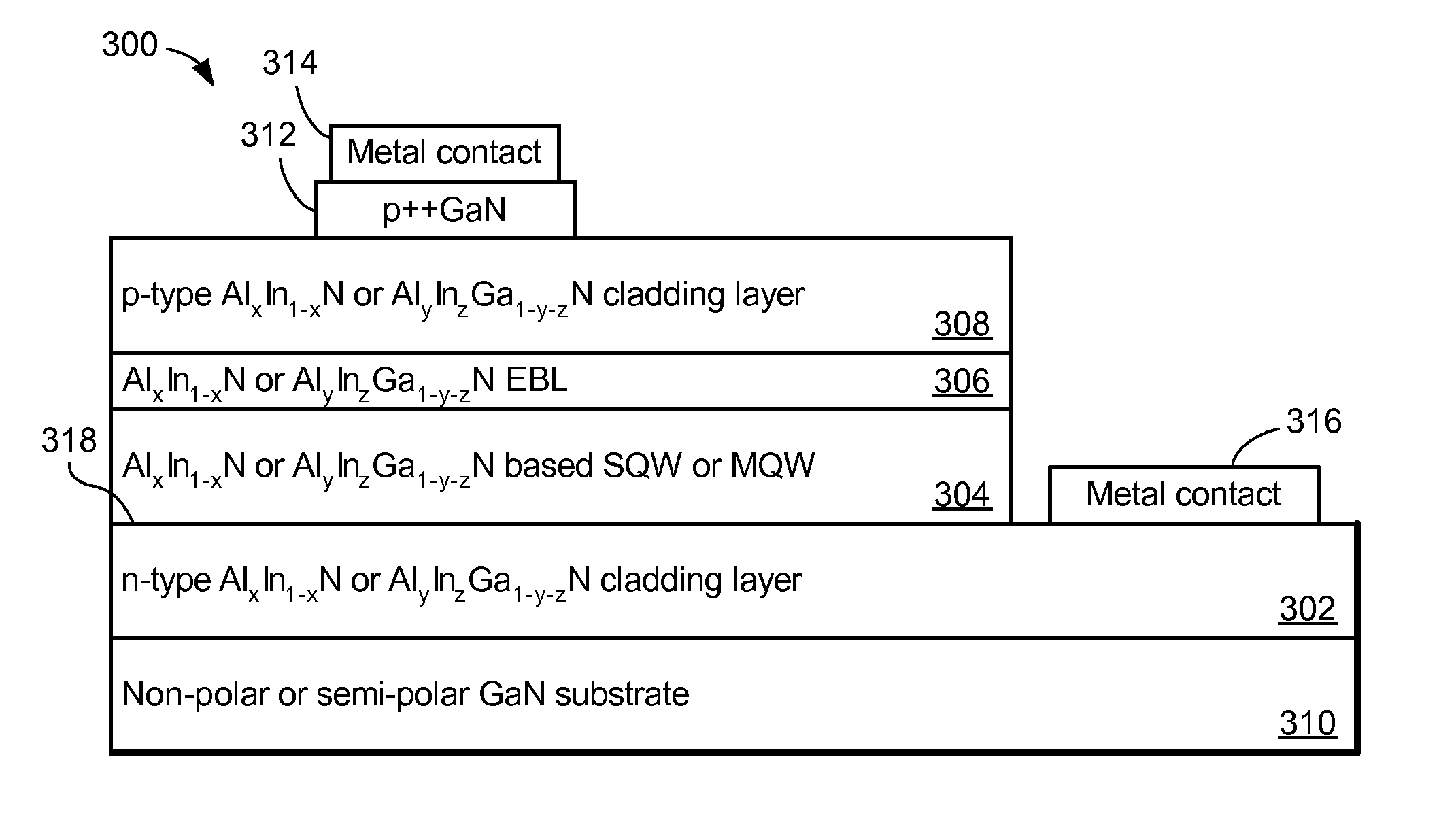
[0029]The present invention describes a device structure that can be utilized for a high-power and high-efficiency LED and LD, in the wavelength ranging from 280 nm to 360 nm, using non-polar or semi-polar AlInN and AlInGaN grown on non-polar or semi-polar GaN. The salient feature of the structure is that the piezoelectric field is reduced, because AlInN and AlInGaN cladding layers can be closely lattice-matched to GaN. In the new structure, the spontaneous polarization is also minimized by growing in non-polar or semi-polar crystal orientations. With the relatively wide bandg...


PUM


Abstract

A high-power and high-efficiency light emitting device with emission wavelength (λpeak) ranging from 280 nm to 360 nm is fabricated. The new device structure uses non-polar or semi-polar AlInN and AlInGaN alloys grown on a non-polar or semi-polar bulk GaN substrate.

Description

CROSS REFERENCE TO RELATED APPLICATION[0001]This application claims the benefit under 35 U.S.C. Section 119(e) of co-pending and commonly-assigned U.S. Provisional Application Ser. No. 61 / 110,449, filed on Oct. 31, 2008, by Roy B. Chung, Zhen Chen, James S. Speck, Steven P. DenBaars, and Shuji Nakamura, entitled “OPTOELECTRONIC DEVICE BASED ON NON-POLAR AND SEMI-POLAR ALUMINUM INDIUM NITRIDE AND ALUMINUM INDIUM GALLIUM NITRIDE ALLOYS,” attorney's docket number 30794.294-US-P1 (2009-258), which application is incorporated by reference herein.BACKGROUND OF THE INVENTION[0002]1. Field of the Invention[0003]This invention relates to nitride-based optoelectronic devices and a method of fabricating the same.[0004]2. Description of the Related Art[0005](Note: This application references a number of different publications as indicated throughout the specification by one or more reference numbers within brackets, e.g., [x]. A list of these different publications ordered according to these re...

Claims


Application Information

Patent Timeline
IPC IPC(8): H01L33/00
CPCB82Y20/00H01L33/16H01L33/32H01S5/2009H01S5/3201H01S5/3211H01S5/34333H01L33/30
Inventor CHUNG, ROY B.CHEN, ZHENSPECK, JAMES S.DENBAARS, STEVEN P.NAKAMURA, SHUJI
Owner RGT UNIV OF CALIFORNIA
Why Eureka
Try Eureka