Method of Fabricating A Fin Field Effect Transistor (FinFET) Device

Inactive Publication Date: 2010-05-06
QUALCOMM INC
View PDF13 Cites 36 Cited by
  • Summary
  • Abstract
  • Description
  • Claims
  • Application Information

AI Technical Summary

Benefits of technology

[0007]A particular advantage provided by at least one of the disclosed embodiments is a simplified dummy structure patterning process due to larger feature sizes for certain field effect transistors (FETs) of

Problems solved by technology

However, removing one fin to yield an odd number of fins is

Method used


Image

  • Method of Fabricating A Fin Field Effect Transistor (FinFET) Device
  • Method of Fabricating A Fin Field Effect Transistor (FinFET) Device
  • Method of Fabricating A Fin Field Effect Transistor (FinFET) Device

Examples


Embodiment Construction

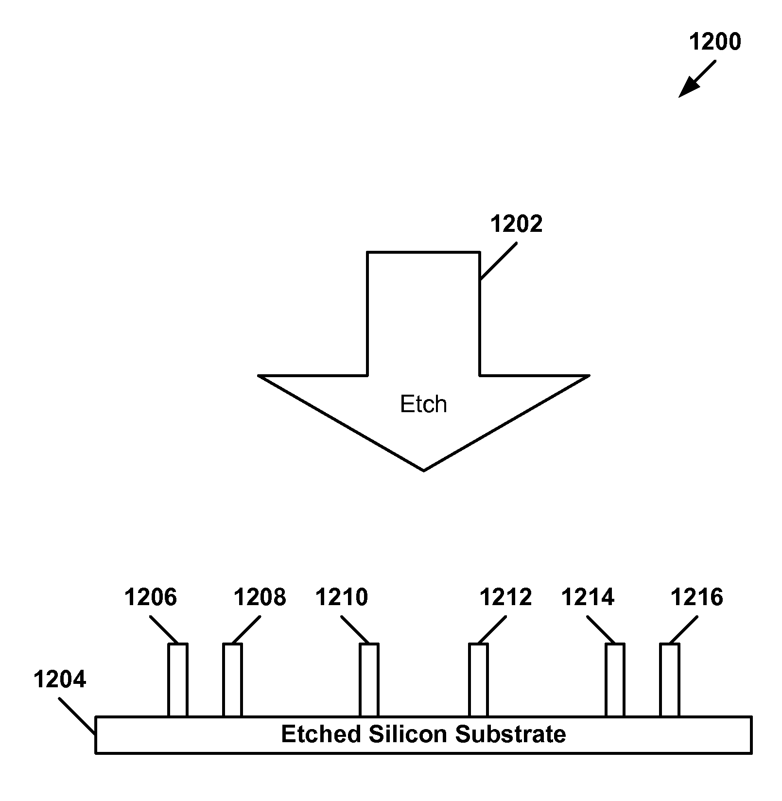
[0024]Referring to FIG. 1, a first illustrative embodiment of a portion of a process to fabricate a fin field effect transistor (FinFET) device is disclosed and generally designated 100. FIG. 1 illustrates a lithographic mask 102 that includes a first window 106, a second window 108, and a third window 110. The lithographic mask 102 may be used to concurrently deposit a first dummy structure 112, a second dummy structure 114, and a third dummy structure 116 on a silicon substrate 104 via a lithography process.

[0025]The first dummy structure 112 has a first width 118, a first sidewall 120 and a second sidewall 122. In an illustrative embodiment, the first sidewall 120 and the second sidewall 122 are first laterally opposed sidewalls. The second dummy structure 114 has a second width 124. In an illustrative embodiment, the second width 124 may be different than the first width 118. For example, the second width 124 may be substantially greater than the first width 118.
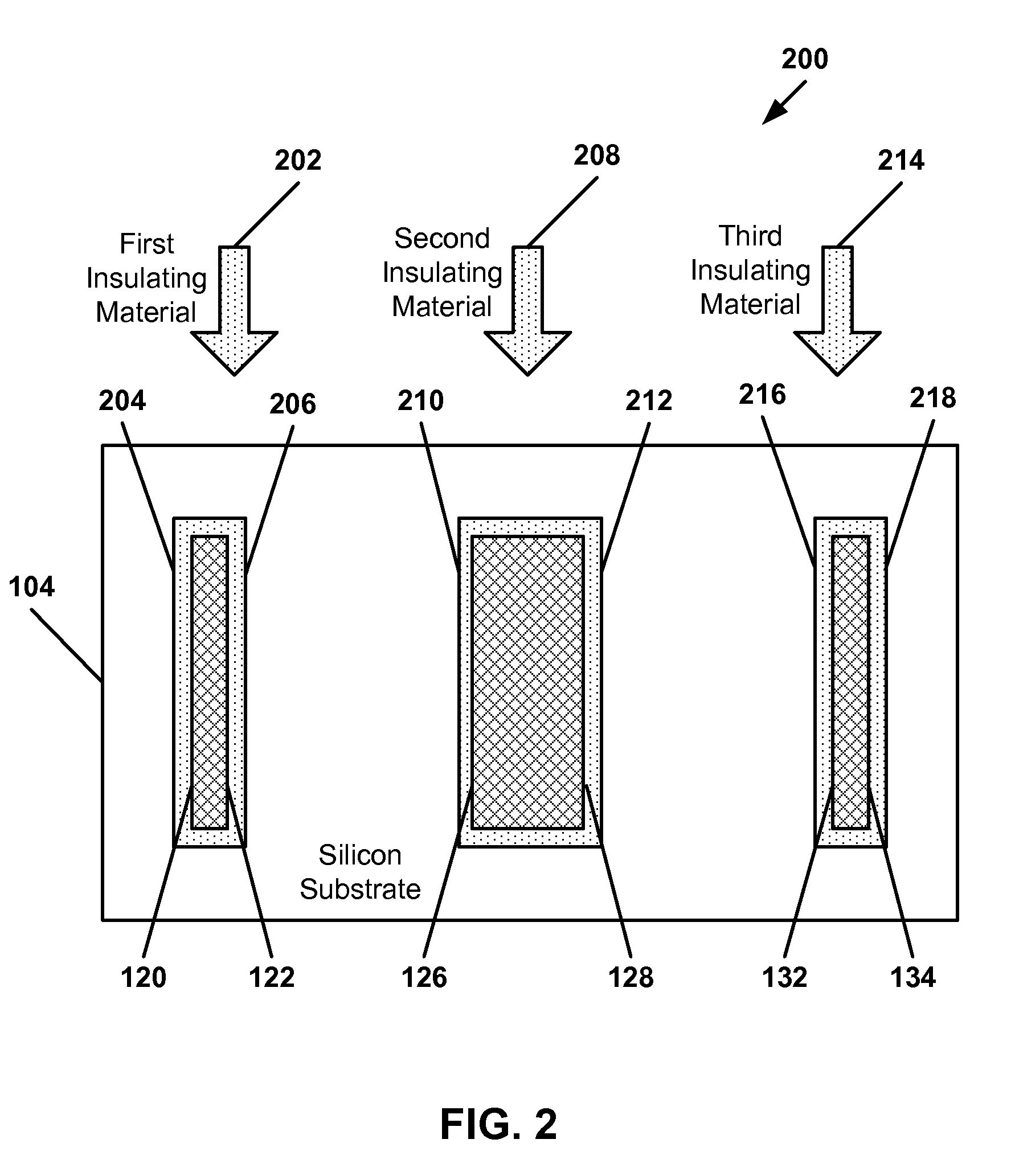
[0026]The second...


PUM


Abstract

A method of fabricating a semiconductor using a fin field effect transistor (FINFET) is disclosed. In a particular embodiment, a method includes depositing, on a silicon substrate, a first dummy structure having a first sidewall and a second sidewall separated by a first width. The method also includes depositing, on the silicon substrate, a second dummy structure concurrently with depositing the first dummy structure. The second dummy structure has a third sidewall and a fourth sidewall that are separated by a second width. The second width is substantially greater than the first width. The first dummy structure is used to form a first pair of fins separated by approximately the first width. The second dummy structure is used to form a second pair of fins separated by approximately the second width.

Description

I. FIELD[0001]The present disclosure is generally related to a method of fabricating a fin field effect transistor (FinFET) device.II. DESCRIPTION OF RELATED ART[0002]Static random access memory (SRAM) bitcells may be implemented using vertical double-gate or tri-gate fin field effect transistors (FinFETs). Using FinFETs enables SRAM bitcells to have one or more benefits over conventional planar Complimentary Metal Oxide Semiconductor (CMOS) technology, such as a smaller bitcell size, a larger cell current, a lower cell leakage current, or a higher static noise margin. FinFETs may be formed using a sidewall transfer method that yields an even number of fins. When the sidewall transfer method is used to fabricate a FinFET device having an odd number of fins, an even number of fins is created and then a fin is removed. However, removing one fin to yield an odd number of fins is a difficult process and requires a high degree of precision.III. SUMMARY[0003]In a particular embodiment, a ...

Claims


Application Information

Patent Timeline
IPC IPC(8): H01L29/78H01L21/336
CPCH01L29/66795H01L29/785H01L21/823431H01L29/41791
Inventor SONG, SEUNG-CHULABU-RAHMA, MOHAMED HASSANHAN, BEOM-MO
Owner QUALCOMM INC
Why Eureka
Try Eureka