Organic electroluminescent device and preparation method thereof
An electroluminescent device, organic technology, applied in the direction of electric solid device, semiconductor/solid state device manufacturing, electrical components, etc., to achieve the effect of small dispersion, reduced preparation process and cost, and increased proportion of forward light output
- Summary
- Abstract
- Description
- Claims
- Application Information
AI Technical Summary
Problems solved by technology
Method used
Image
Examples
preparation example Construction
[0042] A method for preparing an organic electroluminescent device, comprising the following steps:
[0043] S1. On the surface of the roller or the flat plate, the female mold structure is processed by cutting tool engraving or laser ablation;
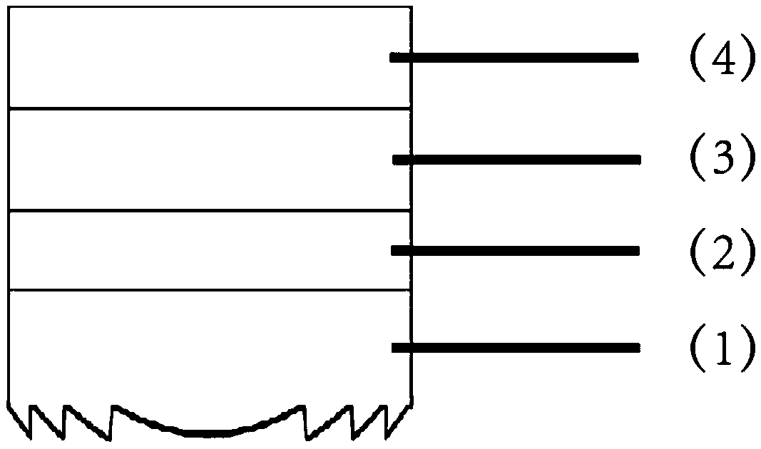
[0044] S2, using the roller or flat plate processed in step S1 to press out the Fresnel lens structure teeth on the base;
[0045] S3, post-processing and shaping the Fresnel lens substrate prepared in step S2;
[0046] S4, using ethanol, acetone ultrasonic and deionized water ultrasonic methods to clean the substrate, and dry after cleaning;
[0047] S5. There is no Fresnel lens structure layer on the substrate, and a transparent conductive film is prepared as a transparent anode, and the square resistance of the transparent anode is 5 to 30 ohms per square;
[0048] S6. Transfer the substrate prepared in step S5 into the vacuum chamber, control the rate of 1-10nm / s, and sequentially prepare organic functional layers by vacuum ther...
Embodiment
[0052] A green organic electroluminescent device, using a knife to carve a Fresnel lens negative mold on the surface of a glass plate, and preparing a Fresnel lens with a focal length of 16 mm and a groove pitch of 0.1 mm on a PET substrate by hot pressing . Indium tin oxide transparent conductive film was prepared on PET substrate by electron beam evaporation method.
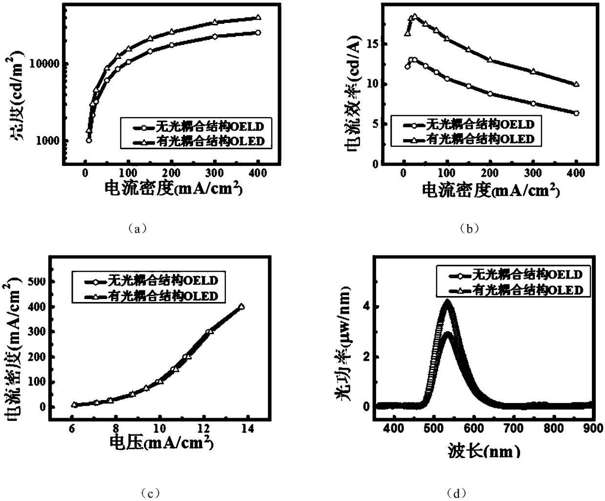
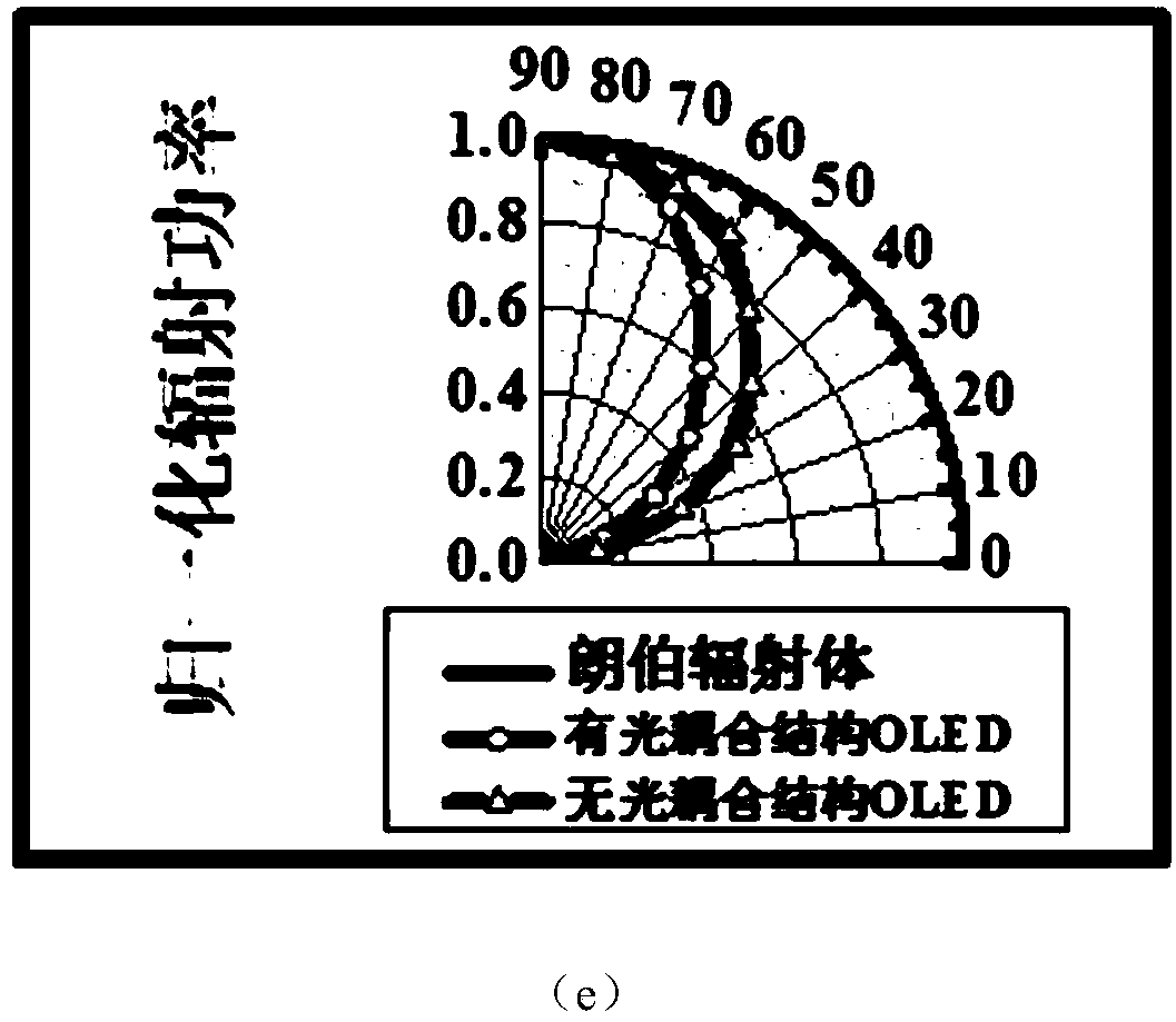
[0053] Prepare organic functional layers sequentially by vacuum thermal evaporation method: 40nm thick 4,4′,4′-Tris[2-naphthyl (phenyl)amino]triphenylamine is the hole injection layer, 20nm thick N,N' -Diphenyl-N,N'-bis(2-naphthyl)-1,1'-biphenyl-4,4'-diamine as hole transport layer, 20 nm thick 8-hydroxyquinoline aluminum doped 10-(2-Benzothiazolyl)-2-,3,6-,7-tetrahydro-1,7-,7-tetramethyl-1H,5H,11H-(1)benzopyranpyran (6,7-8-I, J) Quinolinazine-11-1 was used as the light-emitting layer (the doping volume ratio was 1:0.03), and 40nm-thick 8-hydroxyquinoline aluminum was used as the electron-transporting layer. ...
PUM
 Abstract
Description
Claims
Application Information


