Bumped chip with displacement of gold bumps

a gold bump and chip technology, applied in the field of bumped chips, can solve the problems of bridging between adjacent solder bumps, failure of chip and substrate electrical connection, and inapplicability to fine-pitch flip chip applications, etc., to achieve low cost, high reliability, and lead-free

Inactive Publication Date: 2010-05-06
CHIPBOND TECH
View PDF5 Cites 95 Cited by
  • Summary
  • Abstract
  • Description
  • Claims
  • Application Information

AI Technical Summary

Benefits of technology

[0006]The main purpose of the present invention is to provide a bumped chip with the similar Au bump functions and properties to replace the conve

Problems solved by technology

Since the bonding of conductive bumps between a chip and a substrate are point-to-point electrical connections, any substrate warpage induced by thermal stresses will cause the bumps to break leading to electrical failure between a chip and a substrate.
Currently flip chip technologies can be classified into two major categories, one is solder balls reflowed from solder bumps where solder bumps can not meet the lead-free requirements, moreover, solder bumps can not maintain suitable jointed heights between a chip and a substrate under high temperature reflow leading to bridging between adjacent solder bumps which is not suitable for fine-pitch flip chip applications.
Even though the reliability of Au bumps is good without bridging issues between adjacent Au bumps, however, the material cost of Au bumps is very high, therefore, substitute bumps are

Method used


Image

  • Bumped chip with displacement of gold bumps
  • Bumped chip with displacement of gold bumps
  • Bumped chip with displacement of gold bumps

Examples


Embodiment Construction

[0022]With reference to the attached drawings, the present invention is described by means of the embodiment(s) below where the attached drawings are simplified for illustration purposes only to illustrate the structures or methods of the present invention by describing the relationships between the components and assembly in the present invention. Therefore, the components shown in the figures are not expressed with the actual numbers, actual shapes, actual dimensions, nor with the actual ratio. Some of the dimensions or dimension ratios have been enlarged or simplified to provide a better illustration. The actual numbers, actual shapes, or actual dimension ratios can be selectively designed and disposed and the detail component layouts may be more complicated.

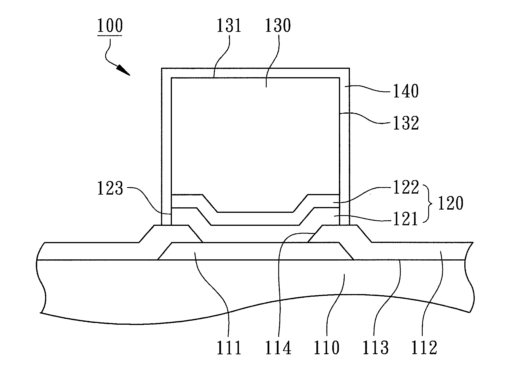
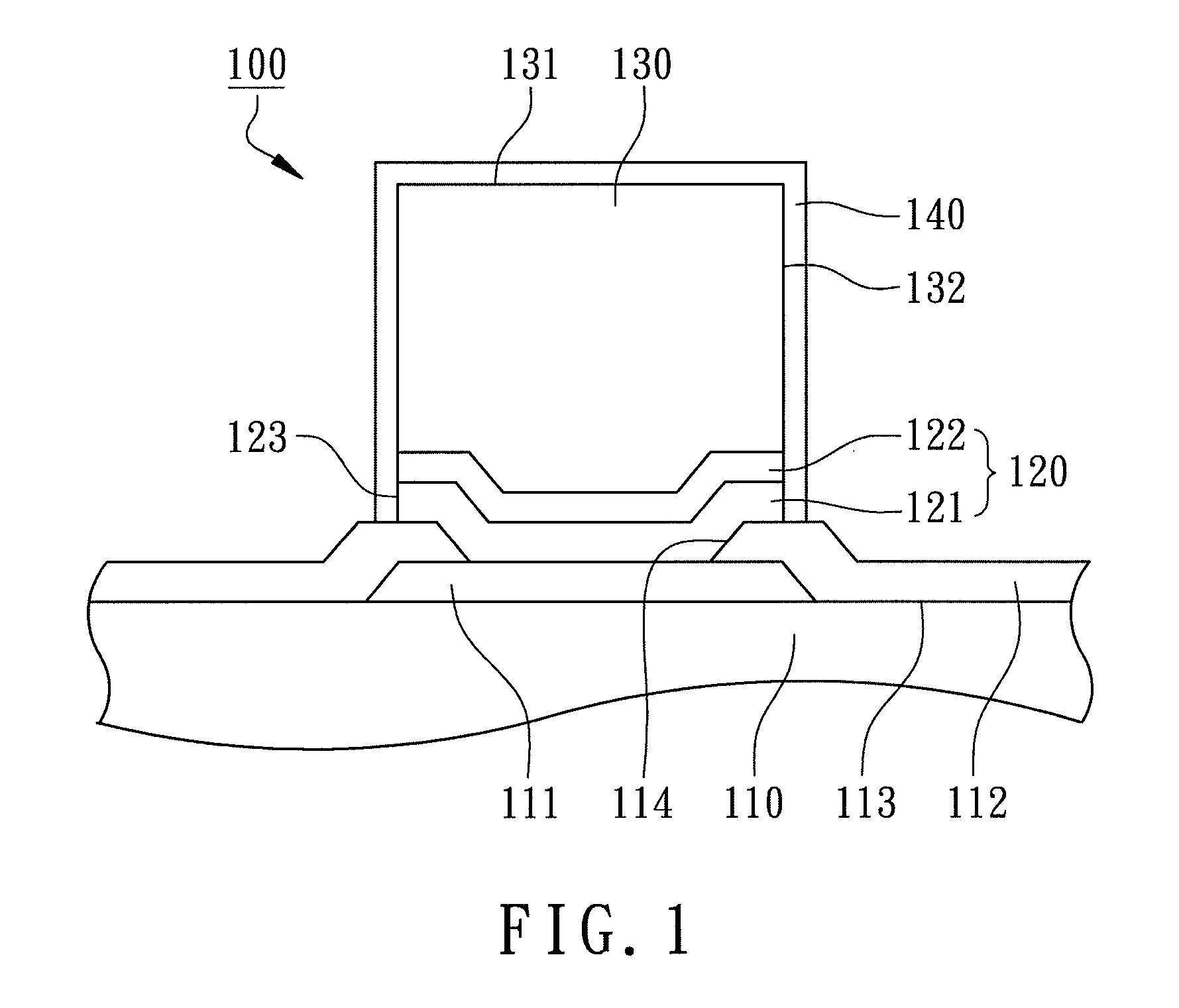
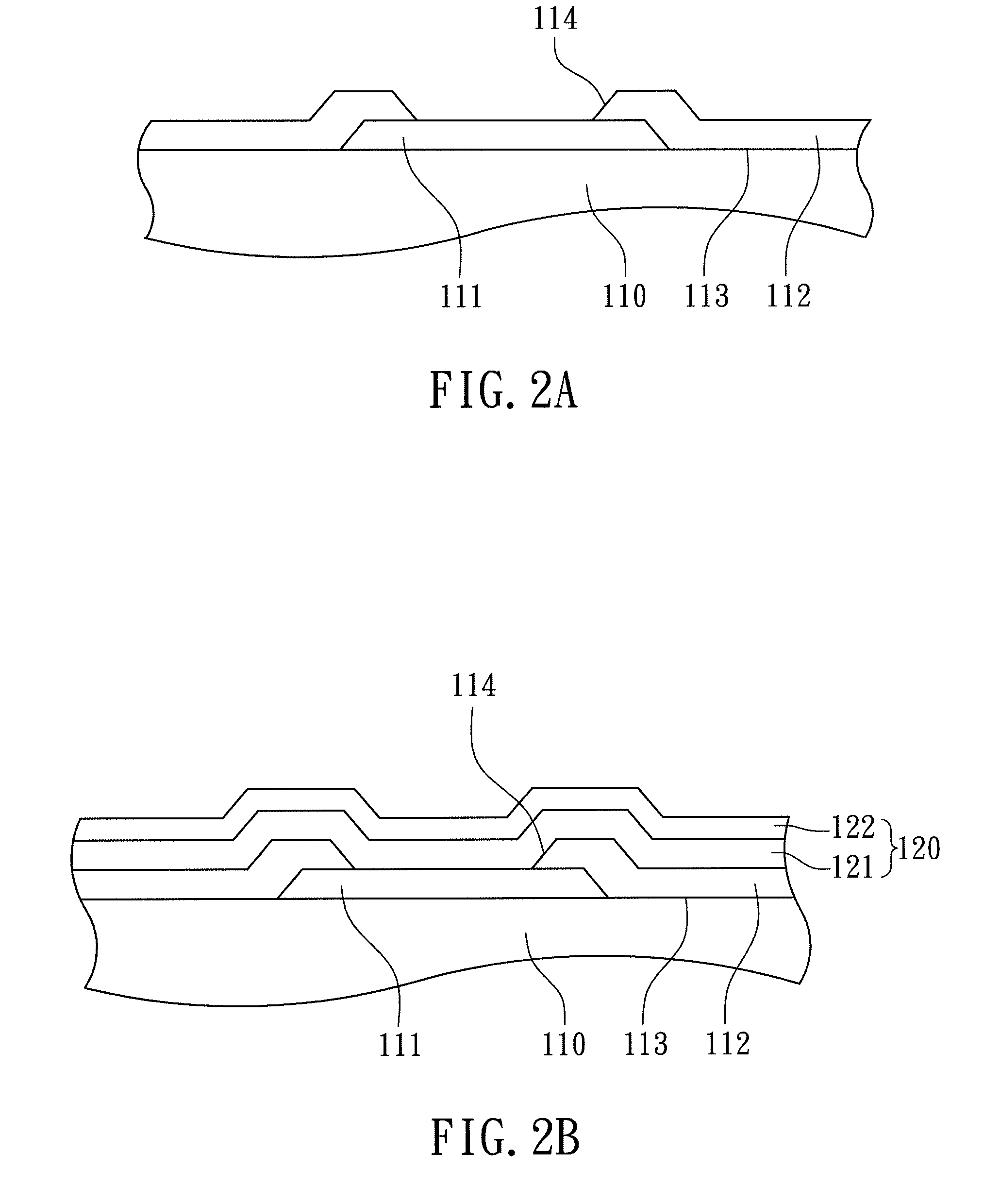
[0023]According to the first embodiment of the present invention, a bumped chip 100 is illustrated in FIG. 1 for a cross-sectional view and from FIG. 2A to FIG. 2F for cross-sectional views of its components during fabricatio...


PUM


Abstract

A bumped chip is revealed, including a chip, a UBM layer, an Ag bump, and a creeping-resist layer. The chip has a bonding pad and a passivation layer covering one surface of the chip and exposing the bonding pad. The UBM layer is disposed on the bonding pad and covers the passivation layer at the peripheries of the opening. The Ag bump is disposed on the UBM layer to form as a pillar bump having a top surface and a pillar sidewall. The creeping-resist layer is formed at least on the pillar sidewall to fully encapsulate the Ag bump. Therefore, the disclosed bumped chip will have no Ag-creeping due to exerting stresses nor changing of joint heights under high temperature environment to meet the bumping requirements of lead-free, high reliability, and lower cost.

Description

FIELD OF THE INVENTION [0001]The present invention relates to semiconductor devices, and more particularly to bumped chips.BACKGROUND OF THE INVENTION[0002]Flip-chip bonding (FC) technology and inner lead bonding (ILB) technology are to dispose a plurality of conductive bumps or extruded electrodes on the bonding pads on the active surface of a chip, then the bumped chip is flipped and bonded to a substrate or the inner leads of a substrate are thermally compressed to the bumped chip to achieve electrical connections. Comparing to the conventional wire-bonding electrical connections, flip chip technology and inner lead bonding technology have shorter electrical paths between a chip and a substrate especially for high I / O density products with better signal qualities with higher operation frequencies.[0003]Since the bonding of conductive bumps between a chip and a substrate are point-to-point electrical connections, any substrate warpage induced by thermal stresses will cause the bum...

Claims


Application Information

Patent Timeline
IPC IPC(8): H01L23/498
CPCH01L2924/01046H01L2924/351H01L2924/01078H01L2924/01079H01L2924/01082H01L2924/10329H01L2924/1433H01L24/11H01L2924/01013H01L2924/01022H01L2924/01029H01L2924/014H01L2924/01006H01L2924/01023H01L2924/01033H01L2224/0345H01L2224/05027H01L2224/13565H01L24/03H01L24/05H01L24/13H01L2224/05166H01L2224/05644H01L2224/11462H01L2224/1147H01L2224/13013H01L2224/13014H01L2224/13023H01L2224/13082H01L2224/13111H01L2224/13139H01L2224/13144H01L2224/13562H01L2224/13583H01L2224/13644H01L2224/13647H01L2224/13655H01L2224/13664H01L2224/73204H01L2224/81191H01L2224/81815H01L2224/83851H01L2224/03912H01L2224/05572H01L2924/01047H01L2224/0401H01L2224/10126H01L2224/13566H01L2924/00013H01L2224/2929H01L2224/293H01L2924/15788H01L2924/0002H01L2224/1308H01L2924/00014H01L2224/13099H01L2224/13599H01L2224/05599H01L2224/05099H01L2224/29099H01L2224/29599H01L2224/05552H01L2924/00
Inventor HO, CHIH-WENHUANG, YUNG-FAWEI, MING-KUOLEE, PO-CHIEN
Owner CHIPBOND TECH
Why Eureka
Try Eureka