Charge sampling device and method

Inactive Publication Date: 2010-05-06
CSEM CENT SUISSE DELECTRONIQUE & DE MICROTECHNIQUE SA RECH & DEV
View PDF4 Cites 4 Cited by
  • Summary
  • Abstract
  • Description
  • Claims
  • Application Information

AI Technical Summary

Benefits of technology

[0013]It is a principle of the invention to provide a temporal sampling device for fast time-varying signals, specifically analog signals, allowing the precise time sampling with very high temporal resolution below one nanosecond.
[0014]A further principle of the invention is to provide a temporal sampling device for recurring, fast time-varying analog signals, allowing the synchronized sampling and accumulation with a very high temporal resolution below one nanosecond.

Problems solved by technology

The temporal characterization of time-varying signals is a problem occurring often in science and technology.
This operation is limited by the speed with which analog signals can be sampled and converted into the corresponding digital representation.
This device requires clocking of the complete CCD line and charge signal sampling at the full sampling frequency, requiring complex, high-performance electronic driving circuitry.
Although the complexity of the clocking circuitry is reduced, it is still necessary to provide a clock with the maximum sampling frequency to the demultiplexing structure, and the two-dimensional CCD charge storage and FISO structures require a substantial amount of space on the sampling device.
However, the method only works for single charge packets, and it is therefore unsuitable to sample analog time signals where the creation and detection of complete trains of charge packets are required.
However, since this transmission line is intended only as a charge transport device, it does not provide any means for the temporal sampling of the charge signals, other than the conventional charge detection circuits which could be placed at the end of the transmission line.

Method used


Image

  • Charge sampling device and method
  • Charge sampling device and method
  • Charge sampling device and method

Examples


Embodiment Construction

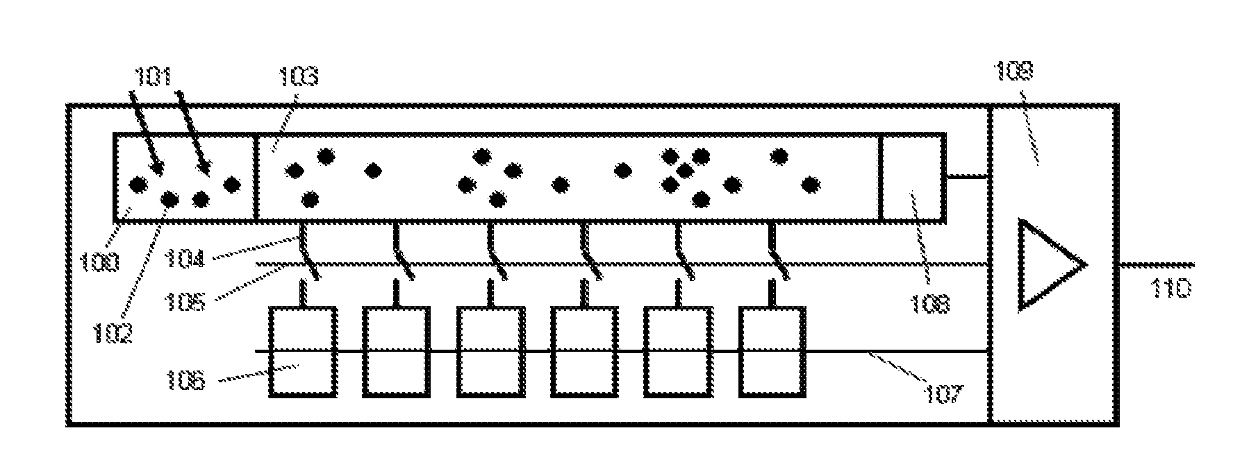
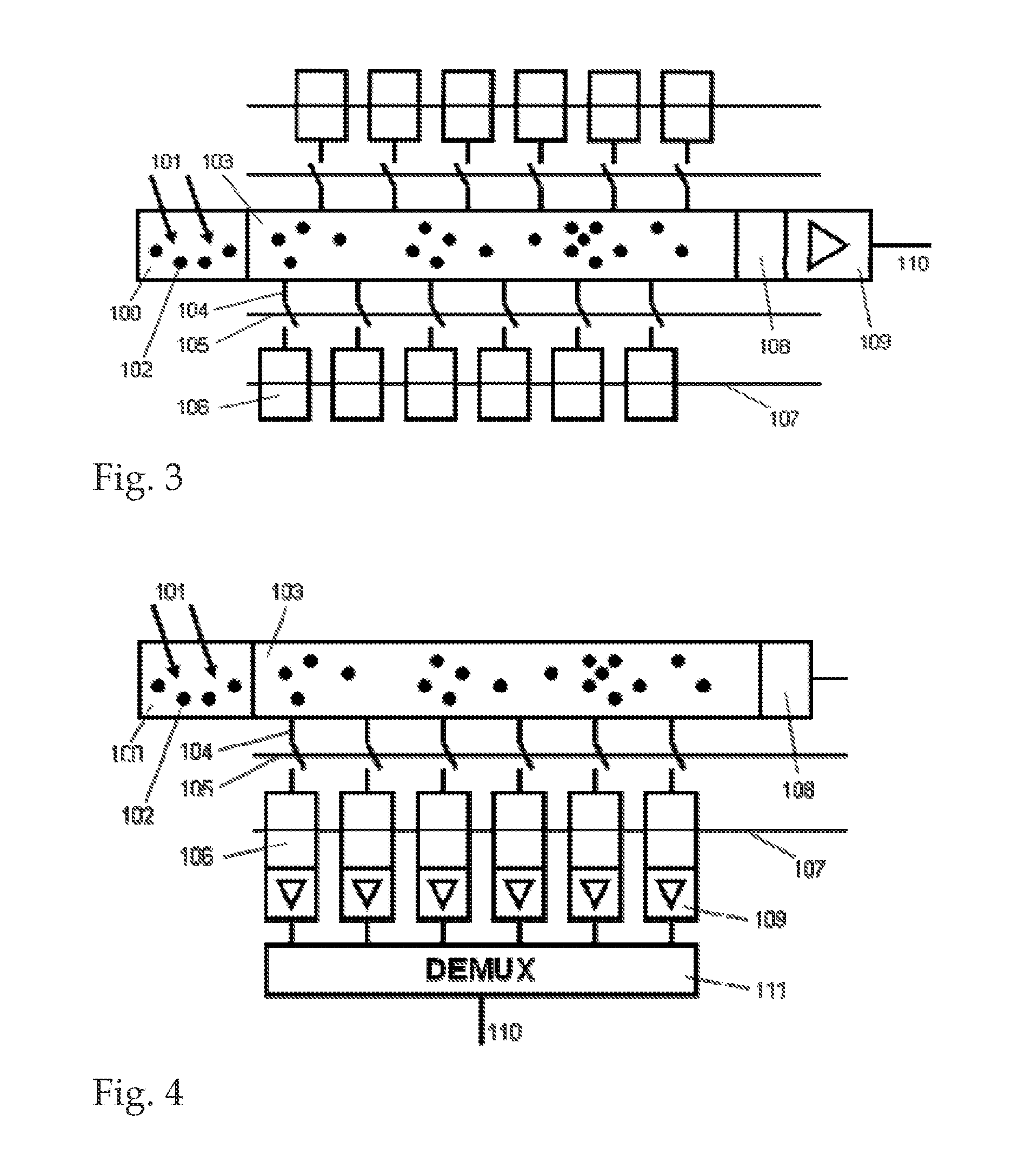
[0078]With reference to FIG. 1, the principle of a signal sampling device according to the present invention is shown on a schematic drawing of an analog signal processing device. This analog signal processing device has of a transducer 100, in which the magnitude of a physical parameter 101 such as temperature; pressure, electromagnetic radiation, particle irradiation, etc. is converted monotonically into a corresponding amount of charge 102. Such transducers are described, for example, by J. Fraden, “Handbook of Modern Sensors: Physics, Designs and Applications”, Springer, Berlin (2004), and they include Seebeck elements (transduction of temperature), charge balances (transduction of force and pressure), photodiodes or charge-coupled devices (transduction of electromagnetic radiation) and ionization chambers (transduction of ionizing and particle radiation).

[0079]Connected to the transducer 100 is a single time conversion element 103 having a longitudinal extension between the tra...


PUM


Abstract

The invention relates to the sampling of temporally changing amounts of charge (102) by receiving varying amounts of charge (102) varying as a function of time, transforming the varying amounts of charge received into a linear distribution pattern, sampling the linear distribution pattern at a plurality of discretely spaced sampling locations (104), and collecting the amounts of charge (102) located between two adjacent scanning locations, and further detecting the collected amounts of charges (102). A temporal sampling device for time-varying analog signals encompasses a transducer (100) in which the analog signals are converted into a corresponding electrical current, a time conversion element (103) in which the electronic charge packets (102) composing the current signal are transported in an electric field along a one-dimensional path, a fast charge-storing and accumulation mechanism with which the charge packets (102) on the one-dimensional path of the time conversion element (103) can all be stored simultaneously, so that their spatial relationship is retained, and a charge detection circuit (109) with which the stored charge packets (102) can be accessed individually and read out with an electronic circuit. In a preferred embodiment, all elements of the sampling device are monolithically integrated using a semiconductor process such as a commercially available CMOS process based on silicon. This makes it possible to provide one- and two-dimensional arrays of such sampling devices, forming line and image sensors.

Description

CROSS-REFERENCE TO RELATED APPLICATION[0001]This application claims priority to EP08168070.4 filed on Oct. 31, 2008, the entirety of each of which is incorporated by this reference.FIELD OF THE INVENTION[0002]This invention relates generally to devices and methods for the temporal sampling of time-varying signals. More specifically, it relates to the temporal sampling of time-varying analog signals, e.g. of signals representing physical quantities such as the intensity of electromagnetic radiation, the pressure of sound waves, the mechanical displacement of objects, or electrical signals such as voltage or current.[0003]The invention relates, in particular, to devices and methods for the sampling of such signals that are changing very rapidly, on a time-scale measured in nanoseconds or below. It further relates to devices and methods for detection of complete trains of charge packets.[0004]The invention further relates to a method of producing such a device, specifically devices for...

Claims


Application Information

Patent Timeline
IPC IPC(8): G01R29/00H04N5/335
CPCG11C19/282G11C19/285G11C27/02G11C27/04
Inventor SEITZ, PETER
Owner CSEM CENT SUISSE DELECTRONIQUE & DE MICROTECHNIQUE SA RECH & DEV
Why Eureka
Try Eureka