Nanodevices for Spintronics and Methods of Using Same

a technology of nanodevices and spintronics, applied in the field of spintronics, can solve the problems of less than an order of magnitude left to go, the progress of miniaturization of traditional solid-state electronics based on manipulating electronic charges rapidly approaching the natural technological limit, and the need for ever-increasing significant challenges

Inactive Publication Date: 2010-05-06
BROOKHAVEN SCI ASSOCS
View PDF6 Cites 42 Cited by
  • Summary
  • Abstract
  • Description
  • Claims
  • Application Information

AI Technical Summary

Benefits of technology

[0016]Preferred embodiments of the present invention can be used to create and control devices based on spin-polarization in the presence of a magnetic field effect induced in a graphene sheet, such as spin-controlled transistors and logic gates, and the like. Active, re-writable, and re-configurable devices can be formed in accordance with the preferred embodiments of the present so that the function of these devices can change depending on the magnetization pattern of an underlying magnetic material.
[0017]Preferred embodiments of the present invention exploit spin-dependent splitting of the electronic bands in graphene based on a magnetic field effect induced in the graphene due to a magnetic proximity effect. The electrical and magnetic properties of devices implemented according to the preferred embodiments of the present invention are advantageously controlled by the magnetization of one or more magnetic materials, so that the graphene-based devices can be tuned and optimized independently. This control can be exploited in a variety of spintronic applications, embodiments of which are described herein.

Problems solved by technology

Progress in the miniaturization of traditional solid state electronics based on manipulating electronic charges is rapidly approaching the natural technological limit imposed by the discrete atomic structure of matter.
Already working at the nanometer scale, current technology not only encounters significant challenges requiring ever-increasing nanoscience research and design effort, but after a more than six order-of-magnitude reduction in size of the electronic components achieved by the beginning of this century, there is less than an order of magnitude left to go.
Hence, there exists not only direct coupling between the two, but also an intricate interplay between magnetic and semiconducting properties, requiring a fine doping / compositional optimization, which has hindered technological progress so far.
Similar material chemistry problems are creating obstacles on the path of using natural semimetals with spin-polarized electronic bands, such as Fe3O4, or La0.7Sr0.3MnO3.
Contacting the graphene sheet with a metallic layer, whether or not part of the device structure, may lead to poorer device performance.

Method used


Image

  • Nanodevices for Spintronics and Methods of Using Same
  • Nanodevices for Spintronics and Methods of Using Same
  • Nanodevices for Spintronics and Methods of Using Same

Examples


Embodiment Construction

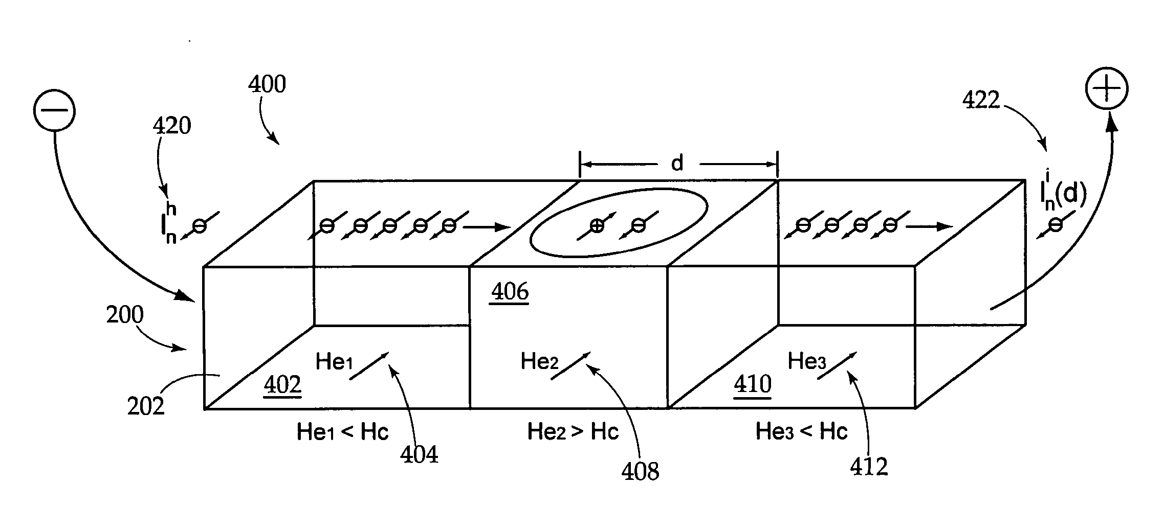
[0024]A suite of electric / logic devices where spin-polarized electric currents are produced and controlled, including spin-polarized diodes, spin-controlled transistors and logic gates, and the like, which are referred to herein as “spintronic devices,” can be realized using the techniques described herein. Such devices may be combined to form active, re-writable and re-configurable devices whose function changes depending on the magnetization pattern written on magnetic media, such as spin-MOSFET and NAND / NOR logic gates.

[0025]The preferred embodiments of the present invention can use graphene-magnet multilayers (GMMs), as described herein, to construct the suite of electric / logic elements by appropriately magnetizing the GMMs. The use of GMMs can be advantageously employed in (re-)writable microchips and processors that can be written from scratch in a magnetic drive, similar to bits of information in magnetic storage devices, and optimized for particular computational tasks as de...


PUM

PropertyMeasurementUnit
thicknessaaaaaaaaaa
temperatureaaaaaaaaaa
temperaturesaaaaaaaaaa

Abstract

Graphene magnet multilayers (GMMs) are employed to facilitate development of spintronic devices. The GMMs can include a sheet of monolayer (ML) or few-layer (FL) graphene in contact with a magnetic material, such as a ferromagnetic (FM) or an antiferromagnetic material. Electrode terminals can be disposed on the GMMs to be in electrical contact with the graphene. A magnetic field effect is induced in the graphene sheet based on an exchange magnetic field resulting from a magnetization of the magnetic material which is in contact with graphene. Electrical characteristics of the graphene can be manipulated based on the magnetization of the magnetic material in the GMM.

Description

[0001]This application claims benefit of U.S. Provisional Application Ser. No. 60 / 892,595 filed Mar. 2, 2007, which is incorporated herein by reference in its entirety.[0002]This invention was made with Government support under contract number DE-AC02-98CH10886, awarded by the U.S. Department of Energy. The Government has certain rights in the invention.BACKGROUND OF THE INVENTION[0003]The invention relates to the field of spintronics and, in particular, to graphene-(antiferro)-ferromagnet multilayers (GMMs) useful in spintronic devices.[0004]Progress in the miniaturization of traditional solid state electronics based on manipulating electronic charges is rapidly approaching the natural technological limit imposed by the discrete atomic structure of matter. Already working at the nanometer scale, current technology not only encounters significant challenges requiring ever-increasing nanoscience research and design effort, but after a more than six order-of-magnitude reduction in siz...

Claims


Application Information

Patent Timeline
Patent Type & Authority Applications(United States)
IPC IPC(8): H03K5/01H01L43/10H01L43/12
CPCB82Y25/00G11C11/16H01L29/1606H01F10/3218H01L29/66984H01F10/005G11C11/161G11C11/18G11C11/1675
Inventor ZALIZNYAK, IGORTSVELIK, ALEXEIKHARZEEV, DMITRI
Owner BROOKHAVEN SCI ASSOCS
Why Eureka
Try Eureka