Semiconductor device and method for manufacturing the semiconductor device

a semiconductor and semiconductor technology, applied in the direction of semiconductor devices, electrical devices, transistors, etc., can solve the problems of element characteristics deteriorating, element characteristics deteriorating, and element characteristics deteriorating in some cases

Active Publication Date: 2010-05-13
SEMICON ENERGY LAB CO LTD
View PDF99 Cites 48 Cited by
  • Summary
  • Abstract
  • Description
  • Claims
  • Application Information

AI Technical Summary

Benefits of technology

[0021]By the surface treatment such as plasma treatment performed before an oxide semiconductor layer is formed over a gate insulating layer, a source electrode layer, and a drain electrode layer, deterioration of element characteristics due to entry of impurities or an oxide film formed on the surfaces of the source electrode layer and the drain electrode layer can be suppressed.

Problems solved by technology

In this case, before the oxide semiconductor layer is formed, element characteristics might deteriorate due to impurities attached to the surfaces of the gate insulating layer, the source electrode layer, and the drain electrode layer.
In addition, if a film including impurities is formed on the surfaces of the gate insulating layer, the source electrode layer, and the drain electrode layer before the oxide semiconductor layer is formed, the element characteristics might deteriorate.
In the case where an oxide semiconductor layer is formed over a source electrode layer and a drain electrode layer which are provided over a gate insulating layer, if the source electrode layer and the drain electrode layer each have a large thickness and unevenness, disconnection of the oxide semiconductor layer formed over the gate insulating layer, the source electrode layer, and the drain electrode layer might occur and the element characteristics might deteriorate in some cases.

Method used


Image

  • Semiconductor device and method for manufacturing the semiconductor device
  • Semiconductor device and method for manufacturing the semiconductor device
  • Semiconductor device and method for manufacturing the semiconductor device

Examples


embodiment 1

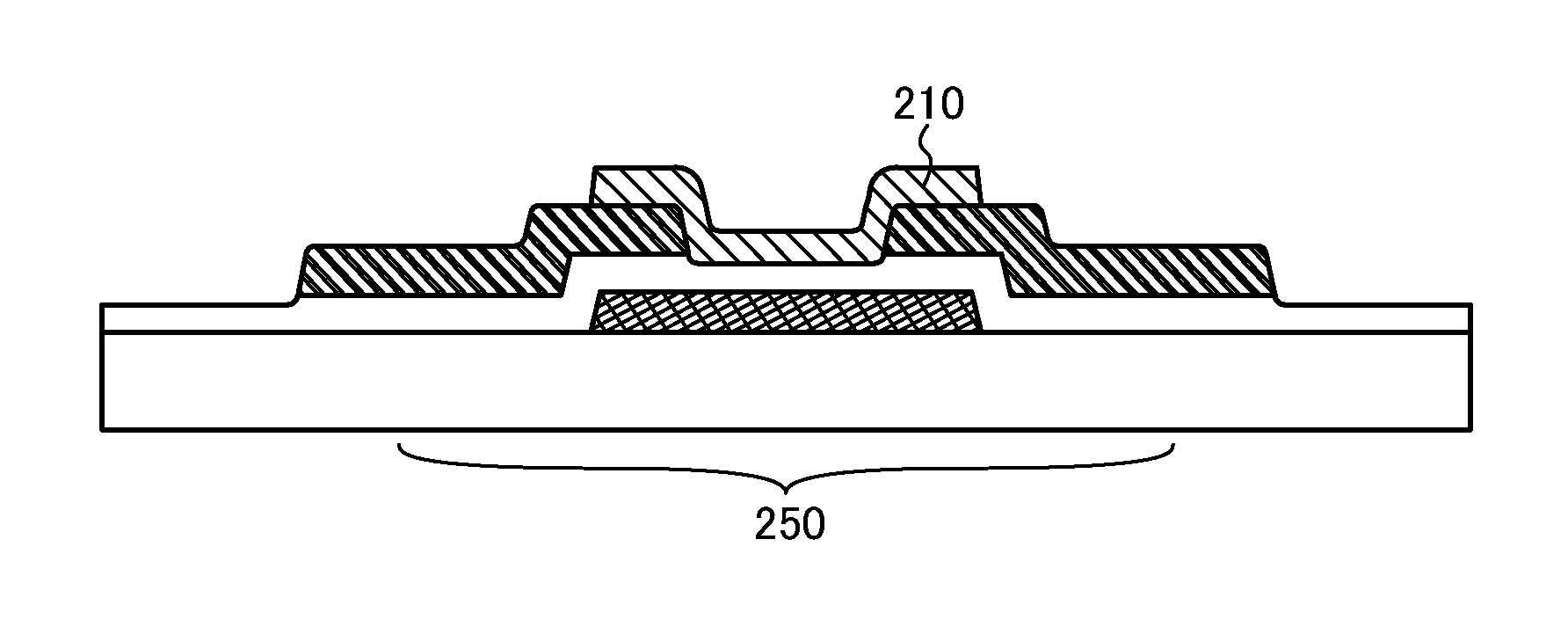
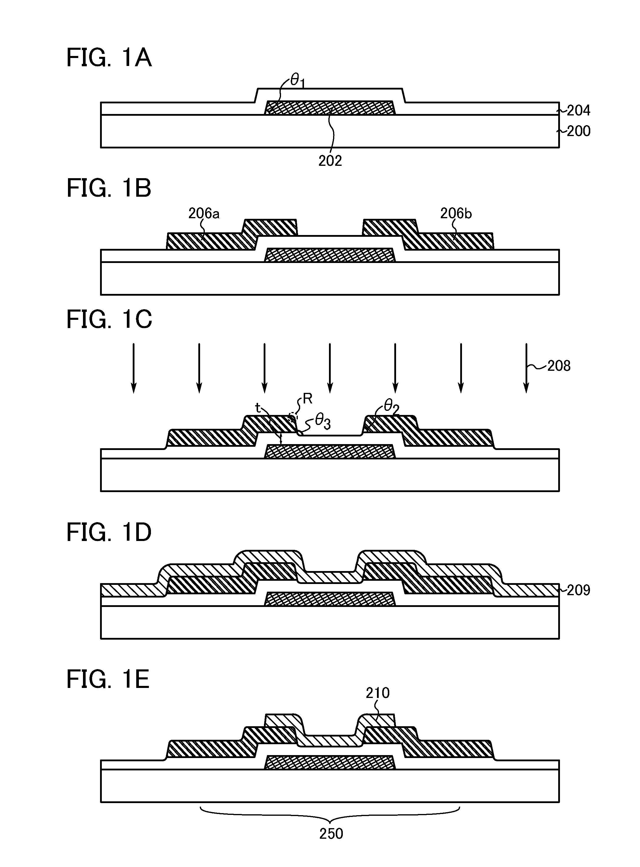
[0048]In this embodiment, an example of a method for manufacturing a semiconductor device which is one mode of the present invention will be described with reference to drawings.

[0049]First, a gate electrode layer 202 is formed over a substrate 200, and then a gate insulating layer 204 is formed over the gate electrode layer 202 (see FIG. 1A).

[0050]As the substrate 200, a substrate having an insulating surface may be used, and for example, a glass substrate can be used. Further, a non-alkali glass substrate is preferable as the glass substrate. As a material of the non-alkali glass substrate, a glass material such as aluminosilicate glass, aluminoborosilicate glass, or barium borosilicate glass is used, for example. In addition, as the substrate 200, an insulating substrate formed using an insulator such as a ceramic substrate, a quartz substrate, or a sapphire substrate; a semiconductor substrate which is formed using a semiconductor material such as silicon and whose surface is co...

embodiment 2

[0099]In this embodiment, a manufacturing process of a semiconductor device which is one mode of the present invention and different from the above embodiment will be described with reference to drawings. Note that the manufacturing process of the semiconductor device in this embodiment has a lot in common with that in Embodiment 1. Thus, description of the common portions is omitted, and differences are described in detail below.

[0100]First, the gate electrode layer 202 is formed over the substrate 200 having an insulating surface, and then the gate insulating layer 204 is formed over the gate electrode layer 202 (see FIG. 3A). For materials and manufacturing methods of the gate electrode layer 202 and the gate insulating layer 204, refer to Embodiment 1.

[0101]Next, a conductive layer 216 is formed over the gate insulating layer 204, and then an oxide semiconductor layer 217 is formed over the conductive layer 216 (see FIG. 3B).

[0102]The conductive layer 216 can be formed by a sput...

embodiment 3

[0138]In this embodiment, a manufacturing process of a display device that is an example of a usage pattern of a semiconductor device, which is one mode of the present invention, will be described with reference to drawings. Note that the manufacturing process described in this embodiment has a lot in common with that in Embodiment 1. Thus, description of the common portions is omitted, and differences are described in detail below. Note that in the following description, FIGS. 5A to 5D and FIGS. 6A to 6D are cross-sectional views, and FIG. 7, FIG. 8, FIG. 9, and FIG. 10 are top views.

[0139]First, a wiring and an electrode (a gate wiring including the gate electrode layer 202, a capacitor wiring 308, and a first terminal 321) are formed over the substrate 200 having an insulating surface (see FIG. 5A and FIG. 7).

[0140]The capacitor wiring 308 and the first terminal 321 can be formed using the same material as that of the gate electrode layer 202. For a material and a manufacturing m...


PUM


Abstract

An object is to suppress deterioration of element characteristics even when an oxide semiconductor is formed after a gate insulating layer, a source electrode layer, and a drain electrode layer are formed. A gate electrode layer is formed over a substrate. A gate insulating layer is formed over the gate electrode layer. A source electrode layer and a drain electrode layer are formed over the gate insulating layer. Surface treatment is performed on surfaces of the gate insulating layer, the source electrode layer, and the drain electrode layer which are formed over the substrate. After the surface treatment is performed, an oxide semiconductor layer is formed over the gate insulating layer, the source electrode layer, and the drain electrode layer.

Description

BACKGROUND OF THE INVENTION[0001]1. Field of the Invention[0002]The present invention relates to a semiconductor device using an oxide semiconductor and a method for manufacturing the semiconductor device.[0003]2. Description of the Related Art[0004]In recent years, a technique in which a thin film transistor (also referred to as a TFT) is formed using an oxide semiconductor and is applied to an electronic device and the like has attracted attention. For example, a technique in which a switching element and the like of an image display device are formed using zinc oxide, an In—Ga—Zn—O-based oxide semiconductor, or the like as an oxide semiconductor layer is disclosed in Reference 1 and Reference 2.[0005]In addition, as a structure of a transistor using an oxide semiconductor layer, various structures are proposed. For example, a bottom-gate bottom-contact structure, in which an oxide semiconductor layer is formed over a source electrode layer and a drain electrode layer which are pr...

Claims


Application Information

Patent Timeline
Patent Type & Authority Applications(United States)
IPC IPC(8): H01L29/786H01L21/336
CPCH01L27/1225H01L29/7869H01L29/41733H01L29/66969H01L29/45H01L29/66742
Inventor AKIMOTO, KENGOTSUBUKU, MASASHI
Owner SEMICON ENERGY LAB CO LTD
Why Eureka
Try Eureka