Organic electroluminescent display device

Inactive Publication Date: 2010-05-13
UDC IRELAND
View PDF7 Cites 187 Cited by
  • Summary
  • Abstract
  • Description
  • Claims
  • Application Information

AI Technical Summary

Benefits of technology

[0030]According to the present invention, an organic EL display device can be provided having a TFT in which a semiconductor with a high field-effect mobility, a high ON/OFF

Problems solved by technology

However, the total efficiency is still low in comparison with the RGB independent emission system.
When the TFTs using a-IGZO are used as driving circuits of display devices for

Method used


Image

  • Organic electroluminescent display device
  • Organic electroluminescent display device
  • Organic electroluminescent display device

Examples


Example

Example 1

1. Production of Organic EL Display Device

1) Formation of Gate Electrode (and Scanning Electric Wires)

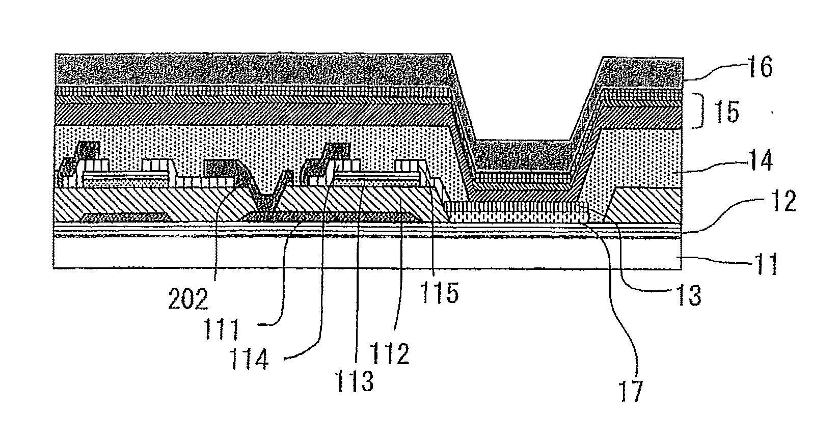
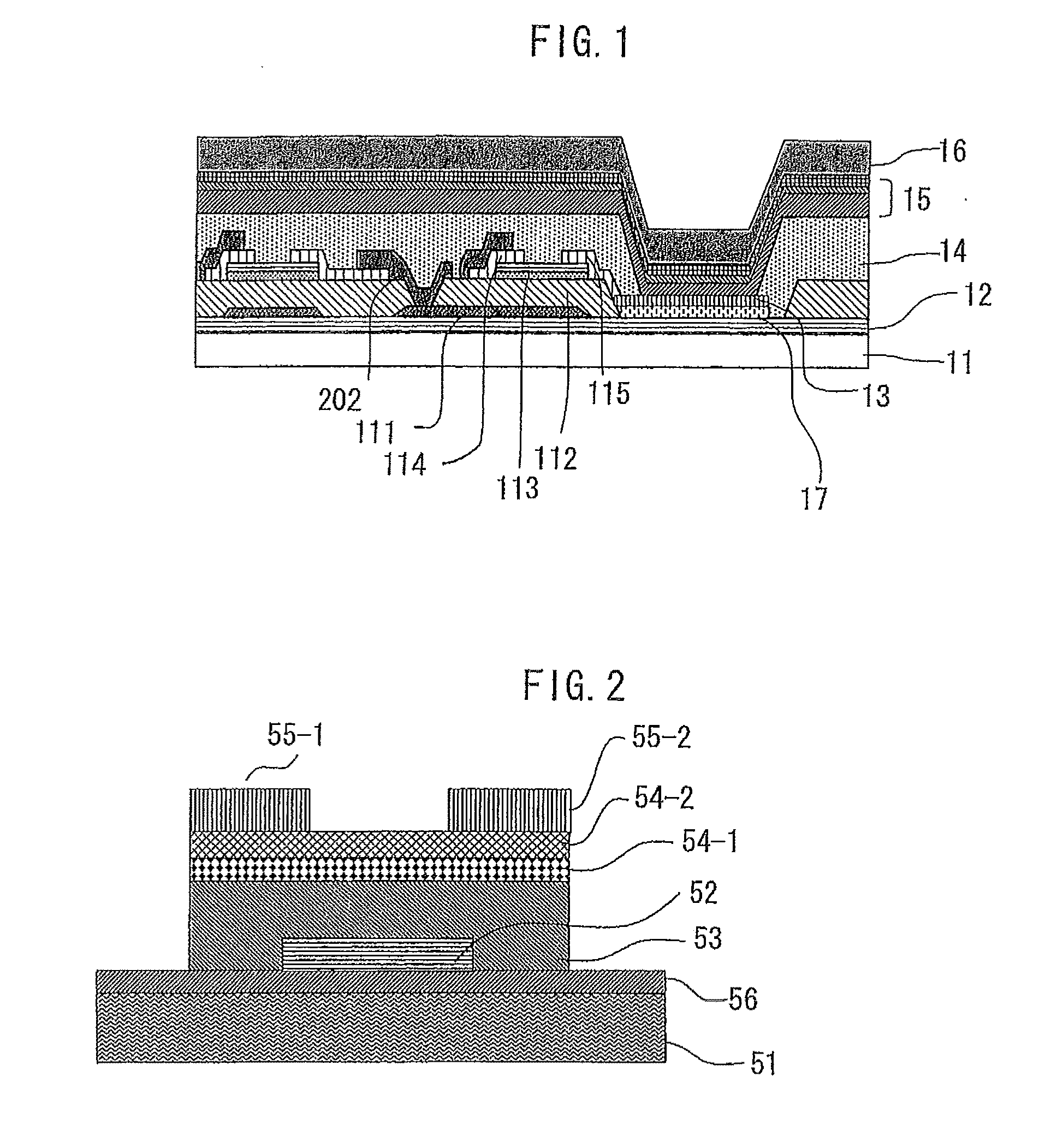
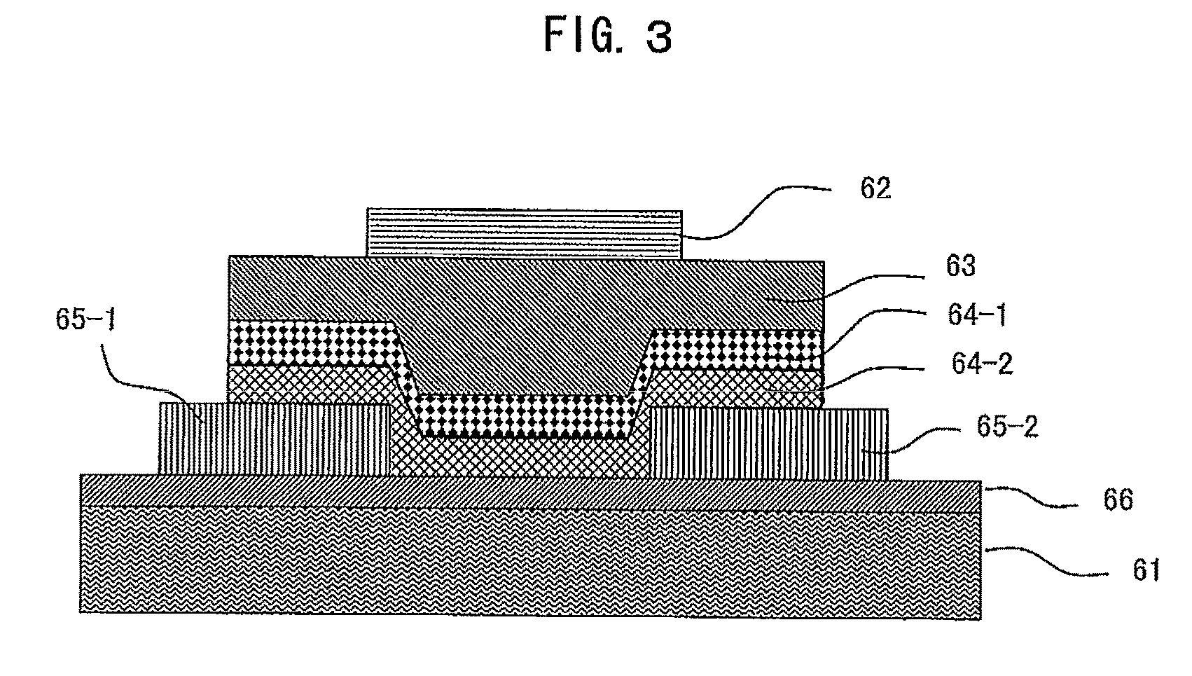
[0199]After a 5 inch×5 inch glass substrate was washed, Mo was deposited to a thickness of 100 nm by sputtering. Then a photoresist was applied, a photomask was superposed thereon, and the photoresist was exposed through the photomask. Unexposed portions were cured by heating, and uncured photoresist was removed by a subsequent treatment with an alkaline developer. Thereafter treatment with an etching liquid was conducted to dissolve and remove that portion of the electrode region that was not covered with the cured photoresist. Finally, the photoresist was peeled off, thereby finishing the patterning process. As a result, a patterned gate electrode and patterned scanning electric wires were formed.

[0200]The treatment conditions at respective steps were as follows:

[0201]Sputtering condition for Mo: Sputtering was conducted by using a DC magnetron sputtering apparatus at a D...

Example

Example 2

[0259]An organic EL display device 2 was prepared in the same manner as in Example 1, except that the substrate size was changed to 15 inch×15 inch size.

[0260]The organic EL display device 2 was evaluated in the same manner as in Example 1, and a high definition emission (200 ppi) at a luminance of 300 cd / m2 was obtained.

Example

Example 3

[0261]An organic EL display device 3 was prepared in the same manner as in Example 2, except that the glass substrate was replaced with a polyethylene naphthalate (PEN) film having a substrate insulating layer.

[0262]The organic EL display device 3 was evaluated in the same manner as in Example 1, and a high definition emission (200 ppi) at a luminance of 300 cd / m2 was obtained.


PUM


Abstract

An organic electroluminescent display device includes at least a driving TFT and pixels which are formed by organic electroluminescent elements and are provided on a substrate of the TFT. The driving TFT includes at least a substrate, a gate electrode, a gate insulating film, an active layer, a source electrode, and a drain electrode. The driving TFT further includes a resistive layer between the active layer and at least one of the source electrode and the drain electrode. The pixels include at least one color-modified pixel which has a color filter that modifies the emission color of the color-modified pixel, and which emits light of the modified color.

Description

TECHNICAL FIELD[0001]The present invention relates to an organic electroluminescent display device having an organic electroluminescent element and a TFT (thin film transistor), in particular to an organic electroluminescent display device having an improved TFT in which an amorphous oxide semiconductor is used and a color-filter-based color-emitting organic electroluminescent element. In the present invention, the TFT refers to a field-effect TFT unless otherwise indicated.BACKGROUND ART[0002]In recent years, flat thin image-display devices (flat panel displays: FPD) have been put into practical use along with advance in technology in liquid crystal and electroluminescence (EL). In particular, organic electroluminescent elements (hereinafter referred to as “organic El elements” in some cases), which use thin-layer materials that are excited by electric current to emit light, can emit light of high luminance with a low voltage, and are expected to realize reduction in the thickness,...

Claims


Application Information

Patent Timeline
IPC IPC(8): G09G5/00H05B44/00
CPCH01L27/322H01L27/3262H05B33/12H01L2251/5338H01L29/7869H10K59/38H10K59/1213H10K2102/311H10K59/126
Inventor MATSUNAGA, ATSUSHINAKAYAMA, MASAYATANAKA, ATSUSHI
Owner UDC IRELAND
Why Eureka
Try Eureka