High density composite focal plane array

a composite and focal plane technology, applied in the field of very large format imaging focal plane arrays, can solve the problems of nitride board substantially lower coefficient of thermal expansion (cte), prior art construction is pushed beyond its size limits, etc., and achieves the effects of low thermal expansion coefficient, high thermal conductivity, and large amount of heat dissipation

Active Publication Date: 2010-05-13
BAE SYST INFORMATION & ELECTRONICS SYST INTERGRATION INC
View PDF40 Cites 10 Cited by
  • Summary
  • Abstract
  • Description
  • Claims
  • Application Information

AI Technical Summary

Benefits of technology

[0007]In accordance with one preferred embodiment of the invention, an aluminum nitride (AlN) board is used in a composite focal plane array. The aluminum nitride board can be fabricated into a multi-layer, two sided circuit card assembly, can be post polished to optically flat tolerances, is structurally stiff and is highly thermally conductive which enables it to dissipate large amounts of heat. Also, the coefficient of thermal expansion of the AlN closely matches that of imaging dice which are constructed out of silicon wafers. However, the aluminum nitride board has substantially lower coefficient of thermal expansion (CTE) than conventional FR-4 and similar fiber glass materials used most commonly for commercial circuit card construction. Additionally, manufacturers of high density backplane connectors typically fabricate their products out of Liquid Crystal Polymer (LCP) or similar materials to more closely match the CTE of the FR-4 and other like materials. In this embodiment of

Problems solved by technology

However, when the size of the imaging plane board is limited, and a large number of imaging die are required, the prior art construction is pushed beyond its limits in terms of size and the number of connections which is achievable by making connections at

Method used


Image

  • High density composite focal plane array
  • High density composite focal plane array
  • High density composite focal plane array

Examples


Embodiment Construction

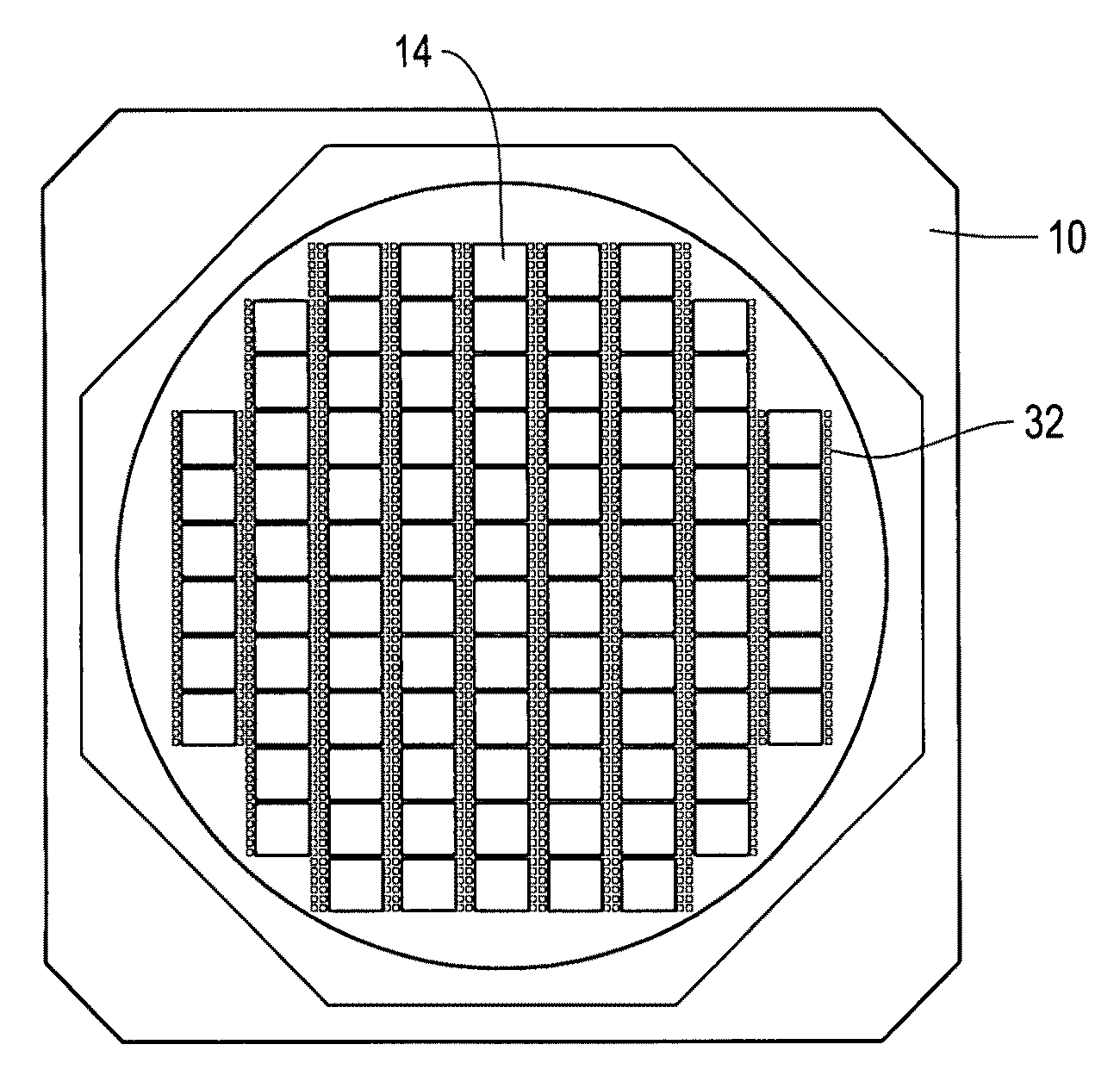
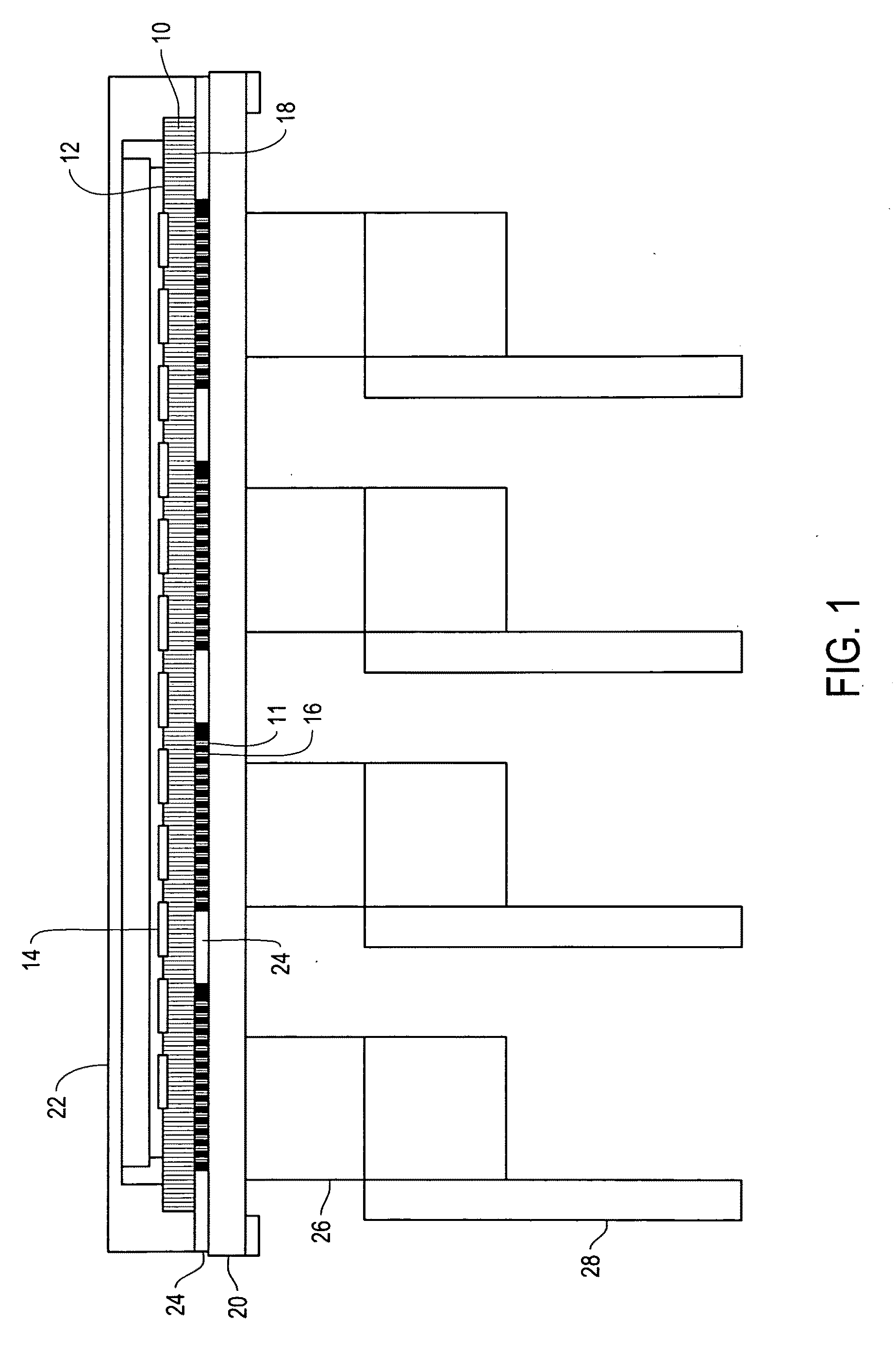
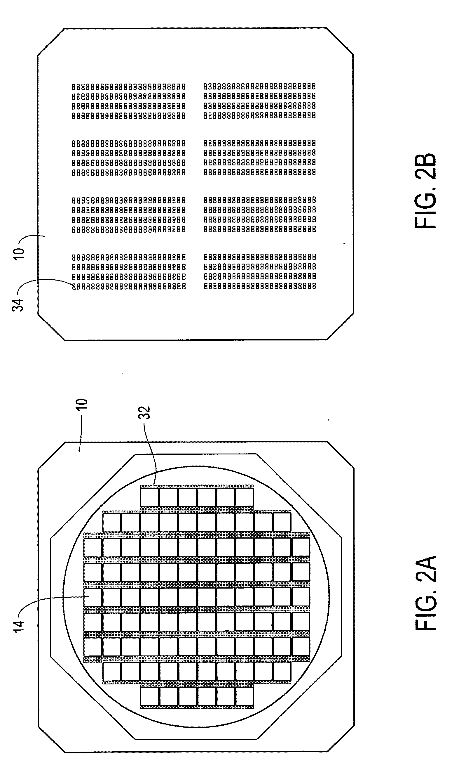
[0022]FIG. 1 shows a cross-sectional view of a high-density composite focal plane array with the integral back plane board and camera control modules. The optically flat focal plane board 10 is preferably made of layers of aluminum nitride. A large number of imaging dies 14 are placed on the top 12 of the board 10. The number of dies may be enough to comprise a gigapixel camera or a quadrant there-off as in this embodiment. Connectors 16 are placed on the bottom side 18 of the focal plane board 10. The connectors 16 connect a back plane motherboard 20 to the focal plane board 10. On top of the entire assembly is a window 22 made of a material such as sapphire. A silicone plate 24 is placed between the imaging plane board and the motherboard and provides a space, which is used to secure the connectors 16. The connectors 16 are sandwiched between the imaging plane board and the FR-4 motherboard 20. The camera assembly, which utilizes the focal plane array and integral back plane array...


PUM


Abstract

A composite focal plane assembly with an expandable architecture has a multi-layer, double-sided aluminum nitride (AlN) substrate and vertical architecture to achieve the dual function of focal plane and electronics backplane. Imaging dice and other electrical components are mounted and wire bonded to one surface and then direct backplane connectivity is provided on the opposing surface through a matrix of electrical contacts. In one embodiment, a flexible connector is sandwiched between the AlN focal plane and a FR-4 backplane is used to compensate for differences in coefficient of thermal expansion (CTE) between the AlN and commercially available high density circuit card connectors that are commonly manufactured from materials with CTE properties more closely approximating FR-4. In an alternate embodiment, the FR-4 and flexible connectors are eliminated by using high density circuit card connectors that are fabricated out of materials more closely matching the CTE of AlN.

Description

FEDERALLY SPONSORED RESEARCH[0001]The present invention was made with United States Government support under Contract No. FA8650-07-C-7732. The United States Government has certain rights in the present invention.TECHNICAL FIELD [0002]The present invention relates to a very large format imaging focal plane array with an expandable architecture that can be used to make a gigapixel camera. More particularly, the invention relates to an apparatus that consolidates the functions of a large scale Focal Plane, signal distribution substrate, heat sink and motherboard into a single planar assembly having a vertical architecture wherein the signal leads from hundreds of active, video and passive components mounted on the top surface of the focal plane are routed through a multi layer, thermally conductive, flat and stiff circuit card substrate to the back surface where the signal lines are formed into a matrix of electrical contacts that can be connected directly or nearly directly to a grou...

Claims


Application Information

Patent Timeline
IPC IPC(8): H04N5/335
CPCH04N5/2253H01L25/065H01L2924/0002H01L2924/00H04N23/54
Inventor SILVA, RAYMOND J.BOWLER, DENNISROBILLARD, GENE
Owner BAE SYST INFORMATION & ELECTRONICS SYST INTERGRATION INC
Why Eureka
Try Eureka