Negative electrode base member
a negative electrode and base member technology, applied in the direction of cell components, sustainable manufacturing/processing, instruments, etc., can solve the problems of insufficient adhesion between the collector and the negative electrode material layer, the degree of deformation tends to increase, and the charge and discharge cycle characteristics of the battery may deteriorate, so as to achieve superior charge and discharge cycle characteristics, high output voltage, and high energy density
- Summary
- Abstract
- Description
- Claims
- Application Information
AI Technical Summary
Benefits of technology
Problems solved by technology
Method used
Image
Examples
first embodiment
Negative Electrode Base Member
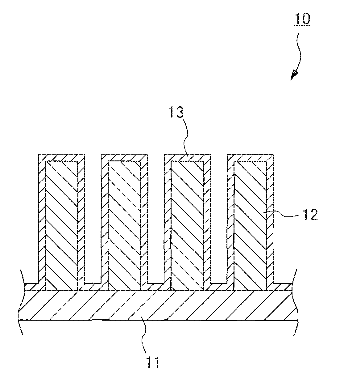
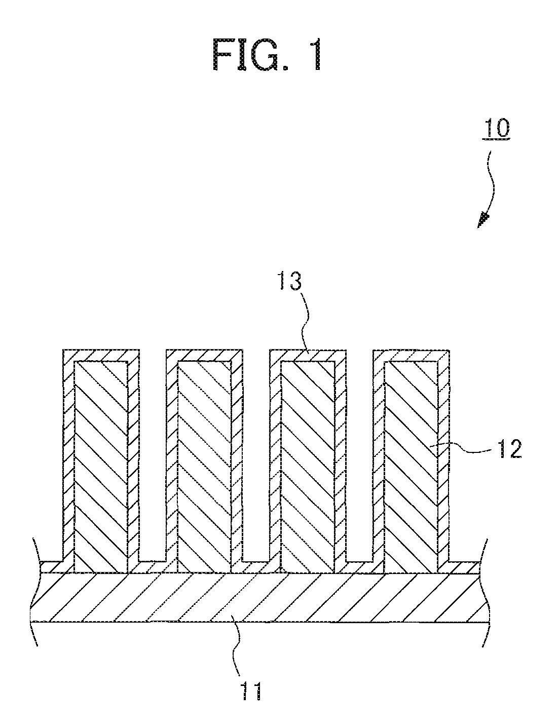
[0024]FIG. 1 shows a schematic view illustrating negative electrode base member 10 according to this embodiment. As is shown in FIG. 1, the negative electrode base member 10 according to this embodiment is composed of support 11, organic film 12, and metal film 13. More specifically, the present invention is characterized by subjecting support 10 having organic film 12 to a plating process to form metal film 13.
Support
[0025]The support 11 for use in the negative electrode base member 10 according to this embodiment is not particularly limited as long as the organic film 12 can be formed on the surface thereof. For example, conventionally well-known substrates such as boards for electronic parts may be used. Specific examples include silicon wafers, silicon wafers having an organic or inorganic antireflection film, silicon wafers on which a magnetic film is formed, boards made of metal such as copper, chromium, iron, or aluminum, glass boards, and the li...
second embodiment
Negative Electrode Base Member
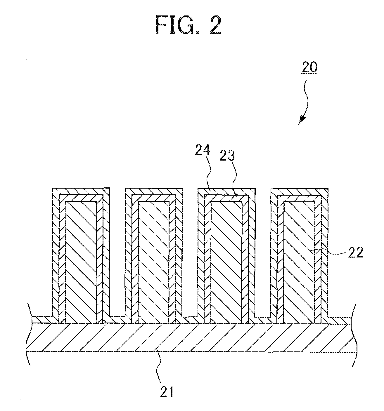
[0191]A schematic drawing of negative electrode base member 20 according to this embodiment is shown in FIG. 2. As shown in FIG. 2, the negative electrode base member 20 according to this embodiment is composed of support 21, organic film 22 covered with metal oxide film 23 on the surface layer, and metal film 24. More specifically, this embodiment is characterized by metal film 24 formed by a plating process on support 21 having organic film 22 covered with metal oxide film 23 on the surface layer.
Support
[0192]The support 21 used in the negative electrode base member 20 according to this embodiment may be similar to that of the first embodiment.
[0193]The organic film 22 of the negative electrode base member 20 according to this embodiment may be formed from an organic compound or an organic resin, and is not particularly limited. Preferably, the organic film 22 may be formed from an organic compound having a hydrophilic group or an organic ...
third embodiment
Negative Electrode Base Member
[0243]A schematic drawing of negative electrode base member 30 according to this embodiment is shown in FIG. 3. As shown in FIG. 3, the negative electrode base member 30 according to this embodiment is composed of support 31, composite film 32, and metal film 33. More specifically, this embodiment is characterized by metal film 33 formed on support 30 having composite film 32.
Support
[0244]The support 31 used in the negative electrode base member 30 according to this embodiment may be similar to that of the first embodiment.
[0245]The composite film 32 in the negative electrode base member 30 according to this embodiment is formed from a composite film-forming material including an organic component such as an organic compound or an organic resin, and an inorganic component such as an inorganic compound or an inorganic resin. Such a composite film-forming material, which is not particularly limited, is preferably a composite film formed from...
PUM
 Abstract
Description
Claims
Application Information


