Wet clean method for semiconductor device fabrication processes

a technology of semiconductor devices and fabrication processes, applied in the preparation of detergent mixtures, detergent compositions, inorganic non-surface active detergent compositions, etc., can solve problems such as dielectric flops, and achieve the effect of reducing or preventing the collapse of patterned features

Inactive Publication Date: 2010-05-20
ADVANCED MICRO DEVICES INC
View PDF3 Cites 45 Cited by
  • Summary
  • Abstract
  • Description
  • Claims
  • Application Information

AI Technical Summary

Problems solved by technology

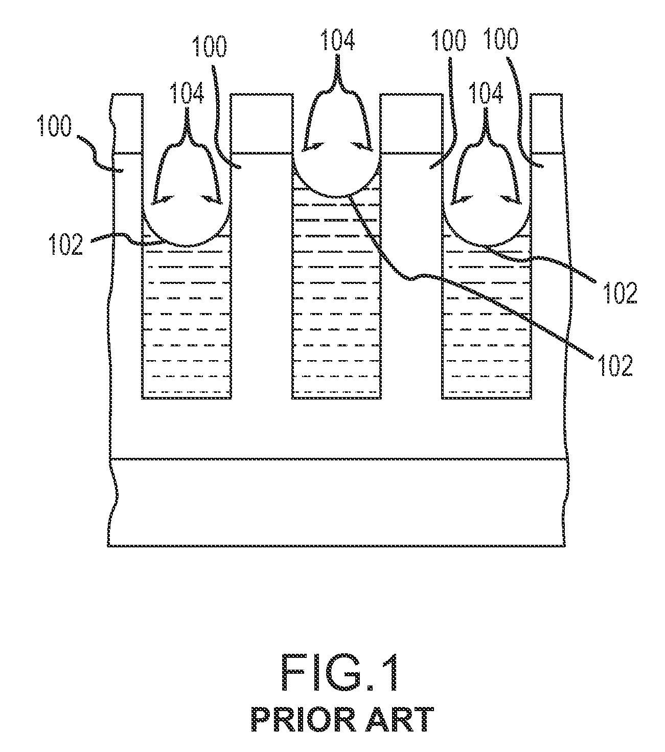
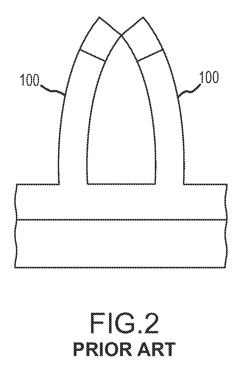
Unfortunately, the problem of dielectric flop worsens as the width and pitch of the features decreases, and worsens as the aspect ratio of the features increases.

Method used


Image

  • Wet clean method for semiconductor device fabrication processes
  • Wet clean method for semiconductor device fabrication processes
  • Wet clean method for semiconductor device fabrication processes

Examples


Embodiment Construction

[0016]The following detailed description is merely illustrative in nature and is not intended to limit the embodiments of the subject matter or the application and uses of such embodiments. As used herein, the word “exemplary” means “serving as an example, instance, or illustration.” Any implementation described herein as exemplary is not necessarily to be construed as preferred or advantageous over other implementations. Furthermore, there is no intention to be bound by any expressed or implied theory presented in the preceding technical field, background, brief summary or the following detailed description.

[0017]For the sake of brevity, conventional techniques related to semiconductor device fabrication may not be described in detail herein. Moreover, the various tasks and process steps described herein may be incorporated into a more comprehensive procedure or process having additional steps or functionality not described in detail herein. In particular, various steps in the manu...


PUM

PropertyMeasurementUnit
widthaaaaaaaaaa
dielectric constantaaaaaaaaaa

Abstract

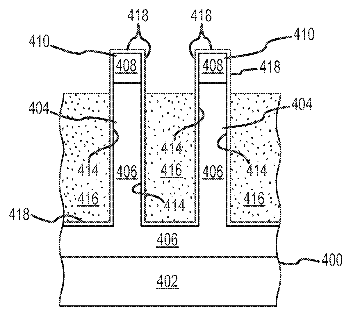
A wet clean method for semiconductor device fabrication begins by providing a semiconductor device structure having a substrate and features protruding from the substrate. The features are formed from a dielectric material, such as an ultra-low-k material. The method continues by cleaning the semiconductor device structure with an aqueous solution and, following the cleaning step, displacing the aqueous solution with a first solvent. Thereafter, the features are exposed to a second solvent that contains a hydrophobic treatment agent that reacts with sidewalls of the features to form a hydrophobic layer on the sidewalls.

Description

TECHNICAL FIELD[0001]Embodiments of the subject matter described herein relate generally to semiconductor device fabrication techniques and processes. More particularly, embodiments of the subject matter relate to wet clean techniques suitable for use during semiconductor device fabrication.BACKGROUND[0002]The majority of present day integrated circuits (ICs) are implemented by using a plurality of interconnected field effect transistors (FETs), which may be realized as metal oxide semiconductor field effect transistors (MOSFETs or MOS transistors). A MOS transistor may be realized as a p-type device (i.e., a PMOS transistor) or an n-type device (i.e., an NMOS transistor). Moreover, a semiconductor device can include both PMOS and NMOS transistors, and such a device is commonly referred to as a complementary MOS or CMOS device. A MOS transistor includes a gate electrode as a control electrode that is formed over a semiconductor substrate, and spaced-apart source and drain regions fo...

Claims


Application Information

Patent Timeline
Patent Type & Authority Applications(United States)
IPC IPC(8): C23G1/00H01L21/31
CPCC11D7/08C11D11/0047H01L21/02063H01L21/76831H01L21/31058H01L21/76814H01L21/3105
Inventor RYAN, E. TODD
Owner ADVANCED MICRO DEVICES INC
Why Eureka
Try Eureka