Method of producing semiconductor device and soq (silicon on quartz) substrate used in the method

a technology of semiconductor devices and substrates, applied in the direction of individual semiconductor device testing, semiconductor/solid-state device testing/measurement, instruments, etc., can solve the problems of very low and the possibility of cracking in the semiconductor device forming region is very low, so as to improve inspection efficiency and reduce the possibility of cracking in the semiconductor device forming region.

Active Publication Date: 2010-05-20
LAPIS SEMICON CO LTD
View PDF5 Cites 87 Cited by
  • Summary
  • Abstract
  • Description
  • Claims
  • Application Information

AI Technical Summary

Benefits of technology

[0012]In the present invention, the crack inspection pattern formed on the SOQ substrate is inspected in the first inspection step. When the crack is detected in the crack inspection pattern, it is determined that there is a possibility of a crack in the semiconductor device forming regions. Accordingly, the semiconductor device forming regions are inspecte

Problems solved by technology

When the crack is detected in the crack inspection pattern, it is determined that there is a possibility of a crack in the semiconductor device forming region

Method used


Image

  • Method of producing semiconductor device and soq (silicon on quartz) substrate used in the method
  • Method of producing semiconductor device and soq (silicon on quartz) substrate used in the method
  • Method of producing semiconductor device and soq (silicon on quartz) substrate used in the method

Examples


first embodiment

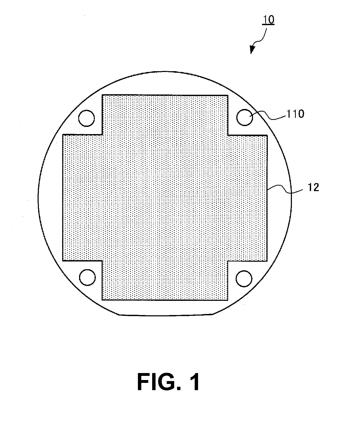
[0020]A first embodiment of the present invention will be explained. FIG. 1 is a schematic plan view showing an SOQ (Silicon On Quartz) substrate 10 according to the first embodiment of the present invention.

[0021]As shown in FIG. 1, the SOQ substrate 10 includes a plurality of semiconductor device forming regions 12 for forming a plurality of semiconductor devices and crack inspection patterns 110.

[0022]In the embodiment, the crack inspection patterns 110 are disposed at four corners of a wafer outside the semiconductor device forming regions 12. When the crack inspection patterns 110 are disposed outside the semiconductor device forming regions 12, it is possible to prevent a crack generated in the crack inspection patterns 110 from reaching the semiconductor device forming regions 12.

[0023]Further, when the crack inspection patterns 110 are disposed at the four corners of the wafer, it is possible to effectively detect a crack over an entire surface of the wafer. For example, whe...

second embodiment

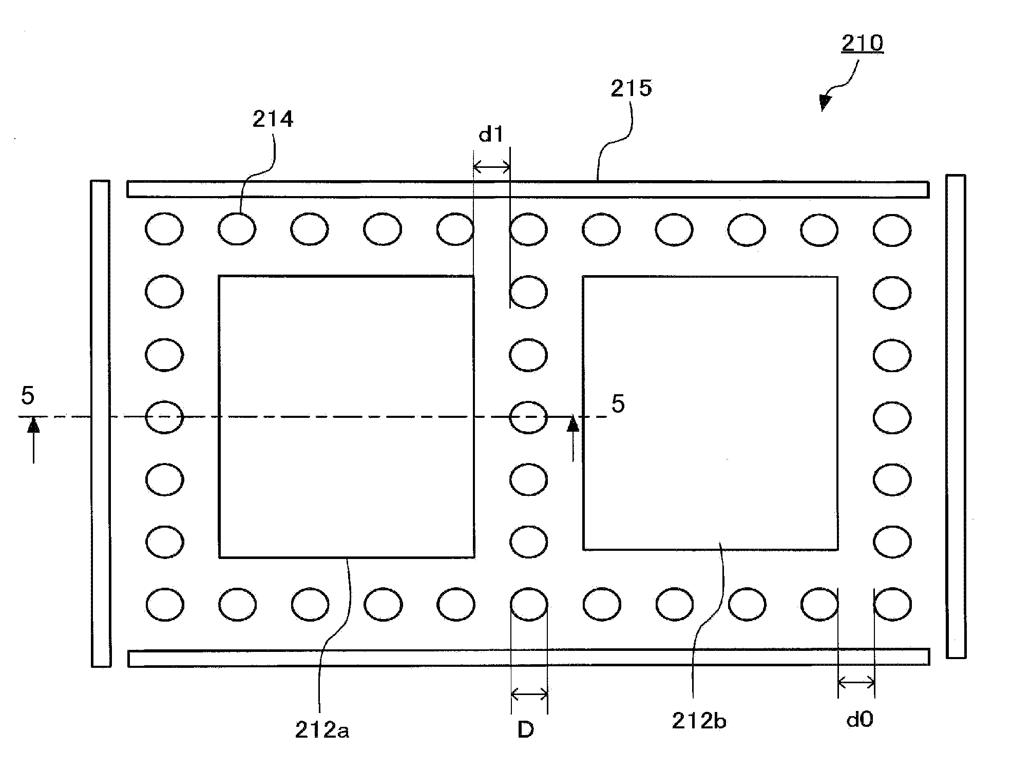
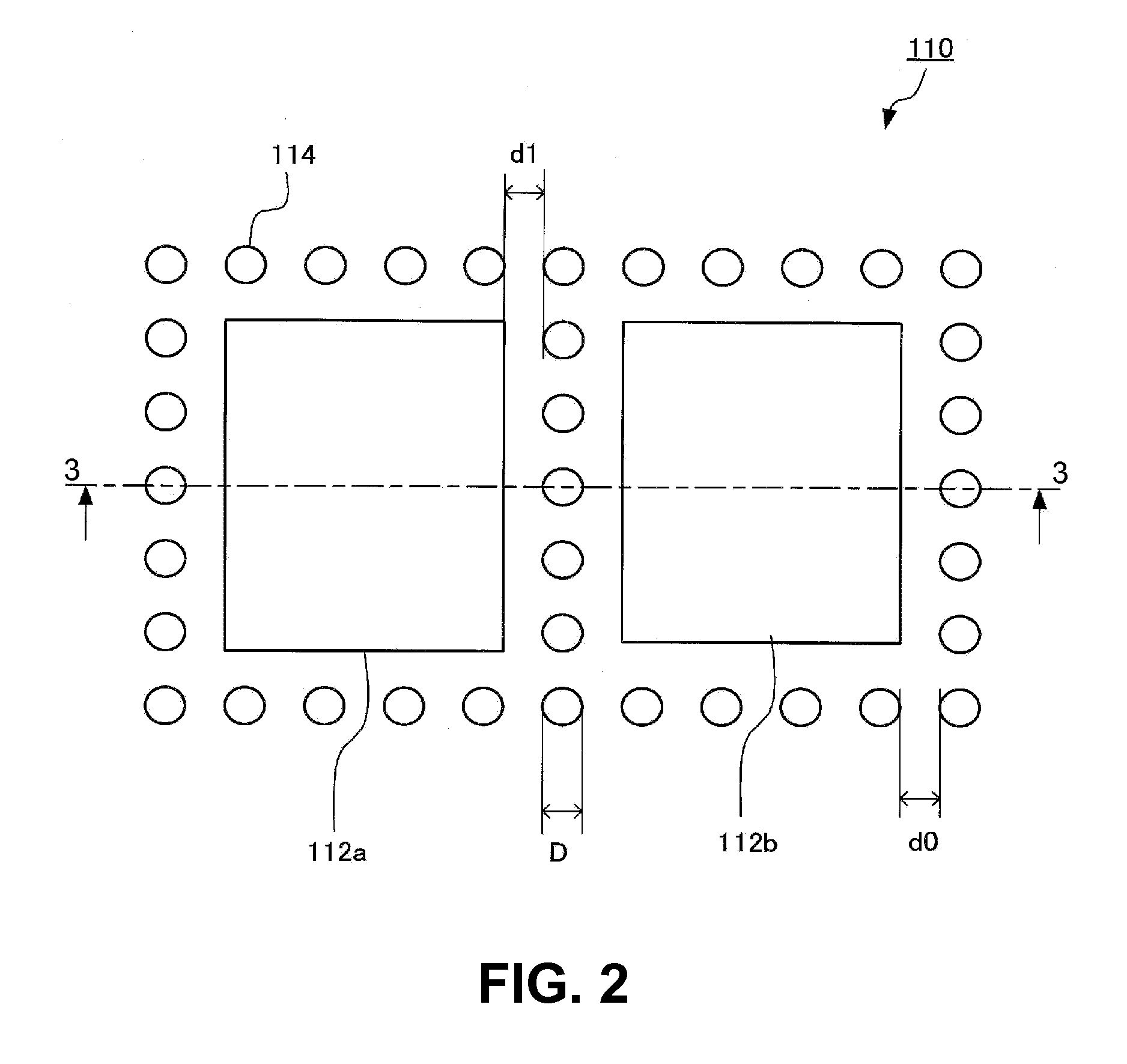
[0033]A second embodiment of the present invention will be explained next. FIG. 4 is a schematic plan view showing a crack inspection pattern 210 according to a second embodiment of the present invention. In the embodiment, the crack inspection patterns 210 have a structure in which a crack is generated more easily than in the semiconductor device forming regions 12.

[0034]More specifically, as shown in FIG. 4, the crack inspection patterns 210 includes large area gates 212a and 212b having an area larger than that of a gate (not shown) to be formed in the semiconductor device forming regions 12. Further, the crack inspection patterns 210 includes a plurality of contacts 214 arranged in parallel near the large area gates 212a and 212b.

[0035]In the embodiment, the large area gates 212a and 212b sandwich one row of the contacts 214. Further, the contacts 214 are arranged to surround circumferences of the large area gates 212a and 212b.

[0036]In the embodiment, as an example, the large...


PUM


Abstract

A method of producing a semiconductor device includes the steps of preparing an SOQ (Silicon On Quartz) substrate in which a semiconductor layer is formed on a quartz substrate; forming a plurality of semiconductor device forming regions in the SOQ substrate; forming a crack inspection pattern in the SOQ substrate; inspecting the crack inspection pattern to detect a crack in the crack inspection pattern in a first inspection step; and inspecting the semiconductor device forming regions to detect a crack in the semiconductor device forming regions in a second inspection step when the crack is detected in the crack inspection pattern in the first inspection step.

Description

BACKGROUND OF THE INVENTION AND RELATED ART STATEMENT[0001]The present invention relates to a method of producing a semiconductor device using an SOQ (Silicon On Quartz) substrate in which a semiconductor layer is formed on a quartz substrate, and to the SOQ substrate used in the method. More specifically, the present invention relates to a method of producing a semiconductor device applicable to a transmission projector and an SOQ substrate used in the method.[0002]A conventional SOQ substrate is formed of a quartz substrate (an insulating substrate) and a silicon layer formed on the quartz substrate. A completely depleted transistor formed of the conventional SOQ substrate provides a low S value and a low substrate floating effect. Further, the completely depleted transistor provides advantages such as a low connection capacity, a high operation speed, low power consumption, and excellent radiation resistance.[0003]Patent Reference has disclosed a structure in which a conventional...

Claims


Application Information

Patent Timeline
IPC IPC(8): H01L21/66H01L23/544
CPCH01L22/12H01L23/544H01L29/78603H01L2924/30105H01L2924/0002H01L27/1218H01L2924/00
Inventor NAGATA, TOSHIO
Owner LAPIS SEMICON CO LTD
Why Eureka
Try Eureka